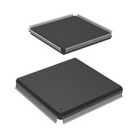
HD6417727F160V Renesas Electronics America, HD6417727F160V Datasheet - Page 598

HD6417727F160V
Manufacturer Part Number
HD6417727F160V
Description
MPU 3V 16K PB-FREE 240-QFP
Manufacturer
Renesas Electronics America
Series
SuperH® SH7700r
Datasheet
1.HD6417727BP100CV.pdf
(1098 pages)
Specifications of HD6417727F160V
Core Processor
SH-3 DSP
Core Size
32-Bit
Speed
160MHz
Connectivity
FIFO, SCI, SIO, SmartCard, USB
Peripherals
DMA, LCD, POR, WDT
Number Of I /o
104
Program Memory Type
ROMless
Ram Size
32K x 8
Voltage - Supply (vcc/vdd)
1.7 V ~ 2.05 V
Data Converters
A/D 6x10b; D/A 2x8b
Oscillator Type
Internal
Operating Temperature
-20°C ~ 75°C
Package / Case
240-QFP
Lead Free Status / RoHS Status
Lead free / RoHS Compliant
Eeprom Size
-
Program Memory Size
-
Available stocks
Company
Part Number
Manufacturer
Quantity
Price
Company:
Part Number:
HD6417727F160V
Manufacturer:
HITACHI
Quantity:
9
Company:
Part Number:
HD6417727F160V
Manufacturer:
Renesas Electronics America
Quantity:
10 000
Part Number:
HD6417727F160V
Manufacturer:
RENESAS/瑞萨
Quantity:
20 000
- Current page: 598 of 1098
- Download datasheet (7Mb)
Section 17 Serial Communication Interface (SCI)
TEND Flag and TE Bit Processing: The TEND flag is set to 1 during transmission of the stop bit
of the last data. Consequently, if the TE bit is cleared to 0 immediately after setting of the TEND
flag has been confirmed, the stop bit will be in the process of transmission and will not be
transmitted normally. Therefore, the TE bit should not be cleared to 0 for at least 0.5 serial clock
cycles (or 1.5 cycles if two stop bits are used) after setting of the TEND flag setting is confirmed.
Receive Error Flags and Transmitter Operation (Clock Synchronous Mode Only): When a
receive error flag (ORER, PER, or FER) is set to 1, the SCI will not start transmitting even if
TDRE is set to 1. Be sure to clear the receive error flags to 0 before starting to transmit. Note that
clearing RE to 0 does not clear the receive error flags.
Receive Data Sampling Timing and Reception Margin in the Asynchronous Mode: In the
asynchronous mode, the SCI operates on a base clock of 16 times the transfer rate frequency. In
receiving, the SCI synchronizes internally with the falling edge of the start bit, which it samples
on the base clock. Receive data is latched on the rising edge of the eighth base clock pulse (figure
17.24).
Rev.6.00 Mar. 27, 2009 Page 540 of 1036
REJ09B0254-0600
data (RxD0)
Synchro-
sampling
sampling
Receive
nization
timing
timing
Basic
clock
Data
Figure 17.24 Receive Data Sampling Timing in Asynchronous Mode
0 1 2 3 4 5 6 7 8 9 10111213 1415 0 1 2 3 4 5 6 7 8 9 10111213 1415 0 1 2 3 4 5
Start bit
8 clocks
16 clocks
−7.5 clocks
+7.5 clocks
D0
D1
Related parts for HD6417727F160V
Image
Part Number
Description
Manufacturer
Datasheet
Request
R

Part Number:
Description:
KIT STARTER FOR M16C/29
Manufacturer:
Renesas Electronics America
Datasheet:

Part Number:
Description:
KIT STARTER FOR R8C/2D
Manufacturer:
Renesas Electronics America
Datasheet:

Part Number:
Description:
R0K33062P STARTER KIT
Manufacturer:
Renesas Electronics America
Datasheet:

Part Number:
Description:
KIT STARTER FOR R8C/23 E8A
Manufacturer:
Renesas Electronics America
Datasheet:

Part Number:
Description:
KIT STARTER FOR R8C/25
Manufacturer:
Renesas Electronics America
Datasheet:

Part Number:
Description:
KIT STARTER H8S2456 SHARPE DSPLY
Manufacturer:
Renesas Electronics America
Datasheet:

Part Number:
Description:
KIT STARTER FOR R8C38C
Manufacturer:
Renesas Electronics America
Datasheet:

Part Number:
Description:
KIT STARTER FOR R8C35C
Manufacturer:
Renesas Electronics America
Datasheet:

Part Number:
Description:
KIT STARTER FOR R8CL3AC+LCD APPS
Manufacturer:
Renesas Electronics America
Datasheet:

Part Number:
Description:
KIT STARTER FOR RX610
Manufacturer:
Renesas Electronics America
Datasheet:

Part Number:
Description:
KIT STARTER FOR R32C/118
Manufacturer:
Renesas Electronics America
Datasheet:

Part Number:
Description:
KIT DEV RSK-R8C/26-29
Manufacturer:
Renesas Electronics America
Datasheet:

Part Number:
Description:
KIT STARTER FOR SH7124
Manufacturer:
Renesas Electronics America
Datasheet:

Part Number:
Description:
KIT STARTER FOR H8SX/1622
Manufacturer:
Renesas Electronics America
Datasheet:

Part Number:
Description:
KIT DEV FOR SH7203
Manufacturer:
Renesas Electronics America
Datasheet:


