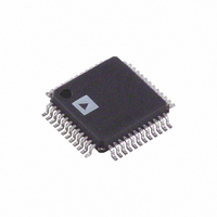
ADUC7032BSTZ-8V-RL Analog Devices Inc, ADUC7032BSTZ-8V-RL Datasheet - Page 86

ADUC7032BSTZ-8V-RL
Manufacturer Part Number
ADUC7032BSTZ-8V-RL
Description
IC BATTERY SENSOR PREC 48-LQFP
Manufacturer
Analog Devices Inc
Series
MicroConverter® ADuC7xxxr
Datasheet
1.ADUC7032BSTZ-8V-RL.pdf
(128 pages)
Specifications of ADUC7032BSTZ-8V-RL
Core Processor
ARM7
Core Size
16/32-Bit
Speed
20.48MHz
Connectivity
LIN, SPI, UART/USART
Peripherals
POR, PSM, Temp Sensor, WDT
Number Of I /o
9
Program Memory Size
96KB (96K x 8)
Program Memory Type
FLASH
Ram Size
6K x 8
Voltage - Supply (vcc/vdd)
3.5 V ~ 18 V
Data Converters
A/D 2x16b
Oscillator Type
Internal
Operating Temperature
-40°C ~ 105°C
Package / Case
48-LQFP
Lead Free Status / RoHS Status
Lead free / RoHS Compliant
Eeprom Size
-
Other names
ADUC7032BSTZ-8V-RLCT
Available stocks
Company
Part Number
Manufacturer
Quantity
Price
Company:
Part Number:
ADUC7032BSTZ-8V-RL
Manufacturer:
Analog Devices Inc
Quantity:
10 000
GENERAL PURPOSE I/O
The ADuC7032 features 9 General Purpose bi-directional I/O
pins (GPIO). In general, many of the GPIO pins have multiple
functions which can be configured by user code. By default, the
GPIO pins are configured in GPIO mode. All GPIO pins have
an internal pull up resistor and their sink capability is 0.8mA
and they can source 0.1mA.
The 9 GPIO are grouped into three ports, Port0, Port1 and
Port2. Port0 is 5 bits wide. Port1 and Port2 are both 2 bits wide.
The GPIO assignment within each port is detailed in Table 48.
A typical GPIO structure is shown Figure 34.
External Interrupts are present on GP0, GP5, GP7 and GP8.
This interrupts are level triggered and are active high. These
interrupts are not latched, therefore the interrupts source must
be present until either IRQSTA or FIQSTA are interrogated.
The Interrupt source must be active for at least 1 CD divided
core clock to guarantee recognition.
Preliminary Technical Data
OUTPUT DRIVE ENABLE
1
GPxDAT[31:24]
GPxDAT[23:16]
OUTPUT DATA
ONLY AVAILABLE ON GP0, GP5, GP7, AND GP8.
GPxDAT[7:0]
INPUT DATA
GPIO IRQ
Figure 34 : ADuC7032 GPIO
Rev. PrD | Page 86 of 128
1
All port pins are configured and controlled by 4 sets (1 set for
each port) of four port specific MMRs:
where x corresponds to the port number 0,1 or 2
During normal operation, user code can control the function
and state of the external GPIO pins via these general purpose
registers. All GPIO pins will retain their external (high or low)
during power-down (POWCON) mode.
GPxCON: Port x Control Register
GPxDAT: Port x Configuration and Data Register
GPxSET: Data set port x
GPxCLR: Data clear port x
REG_DVDD
GPIO
ADuC7032


