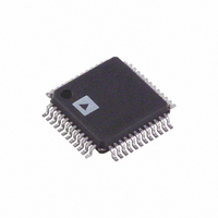
ADUC7032BSTZ-8V-RL Analog Devices Inc, ADUC7032BSTZ-8V-RL Datasheet - Page 88

ADUC7032BSTZ-8V-RL
Manufacturer Part Number
ADUC7032BSTZ-8V-RL
Description
IC BATTERY SENSOR PREC 48-LQFP
Manufacturer
Analog Devices Inc
Series
MicroConverter® ADuC7xxxr
Datasheet
1.ADUC7032BSTZ-8V-RL.pdf
(128 pages)
Specifications of ADUC7032BSTZ-8V-RL
Core Processor
ARM7
Core Size
16/32-Bit
Speed
20.48MHz
Connectivity
LIN, SPI, UART/USART
Peripherals
POR, PSM, Temp Sensor, WDT
Number Of I /o
9
Program Memory Size
96KB (96K x 8)
Program Memory Type
FLASH
Ram Size
6K x 8
Voltage - Supply (vcc/vdd)
3.5 V ~ 18 V
Data Converters
A/D 2x16b
Oscillator Type
Internal
Operating Temperature
-40°C ~ 105°C
Package / Case
48-LQFP
Lead Free Status / RoHS Status
Lead free / RoHS Compliant
Eeprom Size
-
Other names
ADUC7032BSTZ-8V-RLCT
Available stocks
Company
Part Number
Manufacturer
Quantity
Price
Company:
Part Number:
ADUC7032BSTZ-8V-RL
Manufacturer:
Analog Devices Inc
Quantity:
10 000
Preliminary Technical Data
GPIO Port0 Control Register :
Name :
Address :
Default Value :
Access :
Function :
Bit
31-29
28
27-25
24
23-21
20
19-17
16
15-13
12
11-9
8
7-5
4
3-1
0
Description
Reserved
These bits are reserved and should be written as 0 by user code
Reserved
This bit is reserved and should be written as 1 by user code
Reserved
These bits are reserved and should be written as 0 by user code
Internal P0.6 Enable Bit
This bit must be set to 1 by user software to enable the High Voltage Serial Interface before using the HVCON and HVDAT
registered high voltage interface
Reserved
These bits are reserved and should be written as 0 by user code
Internal P0.5 Enable Bit
This bit must be set to 1 by user software to enable the High Voltage Serial Interface before using the HVCON and HVDAT
registered high voltage interface
Reserved
These bits are reserved and should be written as 0 by user code
GPIO4 Function Select Bit
This bit is cleared by user code to 0 to configure the GPIO4 pin as a General Purpose I/O (GPIO) pin
This bit is set to 1 by user code to configure the GPIO4 pin as ECLK enabling a 2.56MHz clock output on this pin
Reserved
These bits are reserved and should be written as 0 by user code
GPIO3 Function Select Bit
This bit is cleared by user code to 0 to configure the GPIO3 pin as a General Purpose I/O (GPIO) pin
This bit is set to 1 by user code to configure the GPIO2 pin as MOSI, Master Output, Slave Input Data for the SPI Port
Reserved
These bits are reserved and should be written as 0 by user code
GPIO2 Function Select Bit
This bit is cleared to 0 by user code to configure the GPIO2 pin as a General Purpose I/O (GPIO) pin
This bit is set to 1 by user code to configure the GPIO3 pin as MISO, Master Input, Slave Output Data for the SPI Port
Reserved
These bits are reserved and should be written as 0 by user code
GPIO1 Function Select Bit
This bit is cleared to 0 by user code to configure the GPIO1 pin as a General Purpose I/O (GPIO) pin
This bit is set to 1 by user code to configure the GPIO1 pin as SCLK, Serial Clock I/O for the SPI Port
Reserved
These bits are reserved and should be written as 0 by user code
GPIO0 Function Select Bit
This bit is cleared to 0 by user code to configure the GPIO0 pin as a General Purpose I/O (GPIO) pin
This bit is set to 1 by user code to configure the GPIO0 pin as SS , Slave Select I/O for the SPI Port
GP0CON
0xFFFF0D00
0x00000000
Read/Write
The 32-bit MMR selects the pin function for each Port0 pin.
Table 49 : GP0CON MMR Bit Designations
Rev. PrD | Page 88 of 128
ADuC7032


