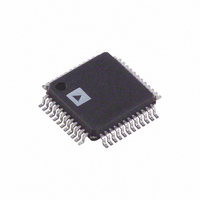
ADUC7032BSTZ-8V-RL Analog Devices Inc, ADUC7032BSTZ-8V-RL Datasheet - Page 90

ADUC7032BSTZ-8V-RL
Manufacturer Part Number
ADUC7032BSTZ-8V-RL
Description
IC BATTERY SENSOR PREC 48-LQFP
Manufacturer
Analog Devices Inc
Series
MicroConverter® ADuC7xxxr
Datasheet
1.ADUC7032BSTZ-8V-RL.pdf
(128 pages)
Specifications of ADUC7032BSTZ-8V-RL
Core Processor
ARM7
Core Size
16/32-Bit
Speed
20.48MHz
Connectivity
LIN, SPI, UART/USART
Peripherals
POR, PSM, Temp Sensor, WDT
Number Of I /o
9
Program Memory Size
96KB (96K x 8)
Program Memory Type
FLASH
Ram Size
6K x 8
Voltage - Supply (vcc/vdd)
3.5 V ~ 18 V
Data Converters
A/D 2x16b
Oscillator Type
Internal
Operating Temperature
-40°C ~ 105°C
Package / Case
48-LQFP
Lead Free Status / RoHS Status
Lead free / RoHS Compliant
Eeprom Size
-
Other names
ADUC7032BSTZ-8V-RLCT
Available stocks
Company
Part Number
Manufacturer
Quantity
Price
Company:
Part Number:
ADUC7032BSTZ-8V-RL
Manufacturer:
Analog Devices Inc
Quantity:
10 000
Bit
31-29
28
27
26
25
24
23-21
Preliminary Technical Data
GPIO Port0 Data Register :
Name :
Address :
Default Value :
Access :
Function :
16
15-5
4
3-1
0
Description
Reserved
These bits are reserved and should be written as 0 by user code
Port 0.4 Direction Select Bit
This bit is cleared to 0 by user code to configure the GPIO pin assigned to P0.4 as an input.
This bit is set to 1 by user code to configure the GPIO pin assigned to P0.4 as an output.
Port 0.3 Direction Select Bit
This bit is cleared to 0 by user code to configure the GPIO pin assigned to P0.3 as an input.
This bit is set to 1 by user code to configure the GPIO pin assigned to P0.3 as an output.
Port 0.2 Direction Select Bit
This bit is cleared to 0 by user code to configure the GPIO pin assigned to P0.2 as an input.
This bit is set to 1 by user code to configure the GPIO pin assigned to P0.2 as an output.
Port 0.1 Direction Select Bit
This bit is cleared to 0 by user code to configure the GPIO pin assigned to P0.1 as an input.
This bit is set to 1 by user code to configure the GPIO pin assigned to P0.1 as an output.
Port 0.0 Direction Select Bit
This bit is cleared to 0 by user code to configure the GPIO pin assigned to P0.0 as an input.
This bit is set to 1 by user code to configure the GPIO pin assigned to P0.0 as an output.
Reserved
These bits are reserved and should be written as 0 by user code
GPIO11 Function Select Bit
This bit is cleared to 0 by user code to internally disable the LIN input data path. In this configuration GPIO11 is used to
support diagnostic read-back on all external high-voltage I/O pins (see HVCFG1[2:0])
This bit is set to 1 by user code to route input data from the LIN interface to both the LIN hardware
timing/synchronization logic and to the UART RxD (receive data). This mode must be configured by user code when
using LIN .
Reserved
These bits are reserved and should be written as 0 by user code
GPIO8 Function Select Bit
This bit is cleared by user code to 0 to configure the GPIO8 pin as a General Purpose I/O (GPIO) pin
This bit is set by user code to 1 to route the LIN input data to the GPIO8 pin. This mode can be used to drive the LIN
transceiver interface as a standalone component without any interaction from MCU or UART.
Reserved
These bits are reserved and should be written as 0 by user code
GPIO7 Function Select Bi
This bit is cleared by user code to 0 to configure the GPIO7 pin as a General Purpose I/O (GPIO) pin
This bit is set by user code to 1 to route data driven into the GPIO7 pin through the on-chip LIN transceiver to be output
at the LIN pin. This mode can be used to drive the LIN transceiver interface as a standalone component without any
interaction from MCU or UART.
GP0DAT
0xFFFF0D20
0x00000000
Read/Write
This 32-bit MMR configures the direction of the GPIO pins assigned to Port0 (see Table 48). This register also sets
the output value for GPIO pins configured as outputs and reads the status of GPIO pins configured as inputs.
Table 52 : GP0DAT MMR Bit Descriptions
Rev. PrD | Page 90 of 128
ADuC7032


