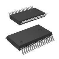
M37542F8FP Renesas Electronics America, M37542F8FP Datasheet - Page 115

M37542F8FP
Manufacturer Part Number
M37542F8FP
Description
IC 740 MCU FLASH 32K 36SSOP
Manufacturer
Renesas Electronics America
Series
740/38000r
Datasheet
1.M37542F8FPU0.pdf
(124 pages)
Specifications of M37542F8FP
Core Processor
740
Core Size
8-Bit
Speed
8MHz
Connectivity
SIO, UART/USART
Peripherals
POR, WDT
Number Of I /o
29
Program Memory Size
32KB (32K x 8)
Program Memory Type
FLASH
Ram Size
1K x 8
Voltage - Supply (vcc/vdd)
2.2 V ~ 5.5 V
Data Converters
A/D 8x10b
Oscillator Type
Internal
Operating Temperature
-20°C ~ 85°C
Package / Case
36-SSOP
Lead Free Status / RoHS Status
Contains lead / RoHS non-compliant
Eeprom Size
-
Available stocks
Company
Part Number
Manufacturer
Quantity
Price
Part Number:
M37542F8FP
Manufacturer:
MIT
Quantity:
20 000
Company:
Part Number:
M37542F8FP#U0
Manufacturer:
TI
Quantity:
109
7542 Group
Notes on Serial I/Oi (i=1, 2)
1. Clock synchronous serial I/O
(1) When the transmit operation is stopped, clear the serial I/Oi
<Reason>
Since transmission is not stopped and the transmission circuit is
not initialized even if only the serial I/Oi enable bit is cleared to “0”
(serial I/Oi disabled), the internal transmission is running (in this
case, since pins TxD
ports, the transmission data is not output). When data is written to
the transmit buffer register in this state, data starts to be shifted to
the transmit shift register. When the serial I/Oi enable bit is set to
“1” at this time, the data during internally shifting is output to the
TxD
(2) When the receive operation is stopped, clear the receive en-
(3) When the transmit/receive operation is stopped, clear both the
<Reason>
In the clock synchronous serial I/O mode, the same clock is used
for transmission and reception.
If any one of transmission and reception is disabled, a bit error oc-
curs because transmission and reception cannot be synchronized.
In this mode, the clock circuit of the transmission circuit also oper-
ates for data reception. Accordingly, the transmission circuit does
not stop by clearing only the transmit enable bit to “0” (transmit
disabled). Also, the transmission circuit cannot be initialized even
if the serial I/Oi enable bit is cleared to “0” (serial I/Oi disabled)
(same as (1)).
(4) When signals are output from the S
(5) When the S
2. UART
When the transmit operation is stopped, clear the transmit enable
bit to “0” (transmit disabled).
<Reason>
Same as (1) shown on the above “1. Clock synchronous serial I/O“.
When the receive operation is stopped, clear the receive enable
bit to “0” (receive disabled).
When the transmit/receive operation is stopped, clear the transmit
enable bit to “0” (transmit disabled) and receive enable bit to “0”
(receive disabled).
Rev.3.03
REJ03B0006-0303
enable bit and the transmit enable bit to “0” (serial I/Oi and
transmit disabled).
able bit to “0” (receive disabled), or clear the serial I/Oi enable
bit to “0” (serial I/Oi disabled).
transmit enable bit and receive enable bit to “0” (transmit and
receive disabled) simultaneously. (any one of data transmis-
sion and reception cannot be stopped.)
side by using an external clock, set all of the receive enable
bit, the S
“1”.
put mode before data is written to the transmit/receive buffer
register.
i
pin and an operation failure occurs.
RDYi
Jul 11, 2008
RDYi
output enable bit, and the transmit enable bit to
signal input is used, set the using pin to the in-
i
, RxD
i
, S
Page 113 of 117
CLKi
, and S
RDYi
RDYi
pin on the reception
function as I/O
Fig. 6 Sequence of setting serial I/Oi control register again
3. Notes common to clock synchronous serial I/O and UART
(1) Set the serial I/Oi (i=1, 2) control register again after the trans-
(2) The transmit shift completion flag changes from “1” to “0” with
(3) When data transmission is executed at the state that an exter-
(4) When the transmit interrupt is used, set as the following se-
<Reason>
When the transmit enable bit is set to “1”, the transmit buffer
empty flag and transmit shift completion flag are set to “1”.
Accordingly, even if the timing when any of the above flags is set
to “1” is selected for the transmit interrupt source, interrupt request
occurs and the transmit interrupt request bit is set.
(5) Write to the baud rate generator (BRGi) while the transmit/re-
Serial I/Oi transmit interrupt enable bit is set to “0” (disabled).
Serial I/Oi transmit enable bit is set to “1”.
more instructions have been executed.
Serial I/Oi transmit interrupt enable bit is set to “1” (enabled).
Serial I/Oi transmit interrupt request bit is set to “0” after 1 or
mission and the reception circuits are reset by clearing both
the transmit enable bit and the receive enable bit to “0.”
Clear both the transmit enable bit (TE)
and the receive enable bit (RE) to “0”
Set the bits 0 to 3 and bit 6 of the
serial I/Oi control register
Set both the transmit enable bit (TE)
and the receive enable bit (RE), or
one of them to “1”
a delay of 0.5 to 1.5 shift clocks. When data transmission is
controlled with referring to the flag after writing the data to the
transmit buffer register, note the delay.
nal clock input is selected as the synchronous clock, set “1” to
the transmit enable bit while the S
to the transmit buffer register while the S
quence.
ceive operation is stopped.
CLKi
is “H” state. Also, write
CLKi
Can be set
with the LDM
instruction at
the same time
is “H” state.


