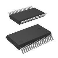
M37542F8FP Renesas Electronics America, M37542F8FP Datasheet - Page 80

M37542F8FP
Manufacturer Part Number
M37542F8FP
Description
IC 740 MCU FLASH 32K 36SSOP
Manufacturer
Renesas Electronics America
Series
740/38000r
Datasheet
1.M37542F8FPU0.pdf
(124 pages)
Specifications of M37542F8FP
Core Processor
740
Core Size
8-Bit
Speed
8MHz
Connectivity
SIO, UART/USART
Peripherals
POR, WDT
Number Of I /o
29
Program Memory Size
32KB (32K x 8)
Program Memory Type
FLASH
Ram Size
1K x 8
Voltage - Supply (vcc/vdd)
2.2 V ~ 5.5 V
Data Converters
A/D 8x10b
Oscillator Type
Internal
Operating Temperature
-20°C ~ 85°C
Package / Case
36-SSOP
Lead Free Status / RoHS Status
Contains lead / RoHS non-compliant
Eeprom Size
-
Available stocks
Company
Part Number
Manufacturer
Quantity
Price
Part Number:
M37542F8FP
Manufacturer:
MIT
Quantity:
20 000
Company:
Part Number:
M37542F8FP#U0
Manufacturer:
TI
Quantity:
109
7542 Group
Table 11 lists the software commands.
After setting the CPU rewrite mode select bit to “1”, execute a soft-
ware command to specify an erase or program operation.
Each software command is explained below.
• Read Array Command (FF
The read array mode is entered by writing the command code
“FF
in one of the bus cycles that follow, the contents of the specified
address are read out at the data bus (D
The read array mode is retained until another command is written.
• Read Status Register Command (70
When the command code “70
the contents of the status register are read out at the data bus (D
to D
The status register is explained in the next section.
• Clear Status Register Command (50
This command is used to clear the bits SR4 and SR5 of the status
register after they have been set. These bits indicate that opera-
tion has ended in an error. To use this command, write the
command code “50
• Program Command (40
Program operation starts when the command code “40
ten in the first bus cycle. Then, if the address and data to program
are written in the 2nd bus cycle, program operation (data program-
ming and verification) will start.
Whether the write operation is completed can be confirmed by
read status register or the RY/BY status flag. When the program
starts, the read status register mode is entered automatically and
the contents of the status register is read at the data bus (D
D
the write operation starts and is returned to “1” upon completion of
the write operation. In this case, the read status register mode re-
mains active until the read array command (FF
Table 11 List of software commands (CPU rewrite mode)
Rev.3.03
REJ03B0006-0303
SRD = Status Register Data
WA = Write Address, WD = Write Data
BA = Block Address to be erased (Input the maximum address of each block.)
7
Read array
Read status register
Clear status register
Program
Block erase
). The status register bit 7 (SR7) is set to “0” at the same time
=
Software Commands
16
7
) by a read in the second bus cycle.
” in the first bus cycle. When an address to be read is input
denotes a given address in the user ROM area.
Jul 11, 2008
Command
16
” in the first bus cycle.
16
)
16
16
)
_____
Page 78 of 117
” is written in the first bus cycle,
0
16
16
to D
)
)
7
).
16
) is written.
Mode
Write
Write
Write
Write
Write
16
” is writ-
First bus cycle
Address
0
(Note 4)
to
0
The RY/BY status flag of the flash memory control register is “0”
during write operation and “1” when the write operation is com-
pleted as is the status register bit 7.
At program end, program results can be checked by reading the
status register.
Fig. 102 Program flowchart
(D
W r i t e
Data
0
FF
70
50
40
20
R e a d s t a t u s r e g i s t e r
to D
16
16
16
16
16
W r i t e “ 4 0
SR4 = “0”?
7
R Y / B Y = “ 1 ” ?
c o m p l e t e d
W r i t e a d d r e s s
W r i t e d a t a
)
P r o g r a m
S R 7 = “ 1 ” ?
S t a r t
o r
Mode
Read
Write
Write
Y E S
Y E S
1 6
”
Second bus cycle
WA (Note 2)
BA (Note 3)
Address
N O
N O
P r o g r a m
SRD (Note 1)
WD (Note 2)
e r r o r
(D
Data
0
D0
to D
16
7
)


