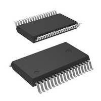
M37542F8FP Renesas Electronics America, M37542F8FP Datasheet - Page 58

M37542F8FP
Manufacturer Part Number
M37542F8FP
Description
IC 740 MCU FLASH 32K 36SSOP
Manufacturer
Renesas Electronics America
Series
740/38000r
Datasheet
1.M37542F8FPU0.pdf
(124 pages)
Specifications of M37542F8FP
Core Processor
740
Core Size
8-Bit
Speed
8MHz
Connectivity
SIO, UART/USART
Peripherals
POR, WDT
Number Of I /o
29
Program Memory Size
32KB (32K x 8)
Program Memory Type
FLASH
Ram Size
1K x 8
Voltage - Supply (vcc/vdd)
2.2 V ~ 5.5 V
Data Converters
A/D 8x10b
Oscillator Type
Internal
Operating Temperature
-20°C ~ 85°C
Package / Case
36-SSOP
Lead Free Status / RoHS Status
Contains lead / RoHS non-compliant
Eeprom Size
-
Available stocks
Company
Part Number
Manufacturer
Quantity
Price
Part Number:
M37542F8FP
Manufacturer:
MIT
Quantity:
20 000
Company:
Part Number:
M37542F8FP#U0
Manufacturer:
TI
Quantity:
109
7542 Group
A/D Converter
The functional blocks of the A/D converter are described below.
[A/D conversion register] AD
The A/D conversion register is a read-only register that stores the
result of A/D conversion. Do not read out this register during an A/
D conversion.
[A/D control register] ADCON
The A/D control register controls the A/D converter.
Bit 2 to 0 are analog input pin selection bits.
Bit 3 is the A/D conversion clock selection bit. When “0” is set to this
bit, the A/D conversion clock is f(X
is 122 cycles of f(X
clock is f(X
Bit 4 is the A/D conversion completion bit. The value of this bit re-
mains at “0” during A/D conversion, and changes to “1” at
completion of A/D conversion.
A/D conversion is started by setting this bit to “0”.
[Comparison voltage generator]
The comparison voltage generator divides the voltage between
AV
[Channel selector]
The channel selector selects one of ports P2
and inputs the voltage to the comparator.
[Comparator and control circuit]
The comparator and control circuit compares an analog input volt-
age with the comparison voltage and stores its result into the A/D
conversion register. When A/D conversion is completed, the con-
trol circuit sets the A/D conversion completion bit and the A/D
interrupt request bit to “1”. Because the comparator is constructed
linked to a capacitor, set f(X
clock is 250 kHz or over during A/D conversion.
As for AD translation accuracy, on the following operating condi-
tions, accuracy may become low.
(1) Since the analog circuit inside a microcomputer becomes sen-
(2) When V
Rev.3.03
REJ03B0006-0303
Notes on A/D converter
SS
sitive to noise when V
voltage, accuracy may become low rather than the case
where V
value..
low temperature may become extremely low compared with
that at room temperature. When the system would be used at
low temperature, the use at V
mended.
and V
IN
REF
REF
) and the A/D conversion time is 61 cycles of f(X
REF
Jul 11, 2008
voltage is lower than [ 3.0 V ], the accuracy at the
by 1024, and outputs the divided voltages.
voltage and Vcc voltage are set up to the same
IN
). When “1” is set to this bit, the A/D conversion
REF
IN
) in order that the A/D conversion
voltage is set up lower than Vcc
Page 56 of 117
IN
)/2 and the A/D conversion time
REF
=3.0 V or more is recom-
7
/AN
7
to P2
IN
0
/AN
).
0
,
Fig. 68 Structure of A/D control register
Fig. 69 Structure of A/D conversion register
b7
Read 8-bit (Read only address 0035
Read 10-bit (read in order address 0036
Note: High-order 6-bit of address 0036
Notes 1: These can be used only for 36 pin version.
(Address 0035
(Address 0036
(Address 0035
2: A/D conversion clock=f(X
only when ceramic oscillation or on-chip oscillator is used.
Select f(X
b0
16
16
16
IN
)
)
)
)/2 when RC oscillation is used.
A/D control register
(ADCON : address 0034
A/D conversion clock selection bit (Note 2)
A/D conversion completion bit
Not used (returns “0” when read)
Analog input pin selection bits
000 : P2
001 : P2
010 : P2
011 : P2
100 : P2
101 : P2
110 : P2
111 : P2
0 : Conversion in progress
1 : Conversion completed
0 : f(X
1 : f(X
b9 b8 b7 b6 b5 b4 b3 b2
b7 b6 b5 b4 b3 b2 b1 b0
b7
b7
b7
IN
IN
0
1
2
3
4
5
6
7
)/2
)
IN
16
/AN
/AN
/AN
/AN
/AN
/AN
/AN
/AN
) can be used
)
0
1
2
3
4
5
6
7
16
(Note 1)
(Note 1)
16
, 0035
returns “0” when read.
16
16
, initial value: 10
)
b9 b8
b0
b0
b0
16
)


