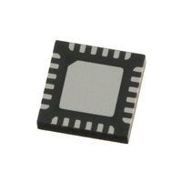
AK5701VNP AKM Semiconductor Inc, AK5701VNP Datasheet - Page 23

AK5701VNP
Manufacturer Part Number
AK5701VNP
Description
IC ADC AUDIO STER 16BIT 24QFN
Manufacturer
AKM Semiconductor Inc
Type
ADCr
Datasheet
1.AK5701VNP.pdf
(64 pages)
Specifications of AK5701VNP
Resolution (bits)
16 b
Sampling Rate (per Second)
7.35k ~ 48k
Data Interface
I²S, Serial
Voltage Supply Source
Analog and Digital
Voltage - Supply
3V
Operating Temperature
-30°C ~ 85°C
Mounting Type
Surface Mount
Package / Case
24-WFQFN Exposed Pad
Lead Free Status / RoHS Status
Lead free / RoHS Compliant
Other names
974-1039-2
AK5701VNP
AK5701VNP
Available stocks
Company
Part Number
Manufacturer
Quantity
Price
Company:
Part Number:
AK5701VNP-L
Manufacturer:
AKM Semiconductor Inc
Quantity:
1 874
Company:
Part Number:
AK5701VNP-L
Manufacturer:
ST
Quantity:
7 190
When PLL reference clock input is EXLRCK or EXBCLK pin, the sampling frequency is selected by FS3 and FS2 bits
(Table
■
1) PLL Master Mode (PMPLL bit = “1”, M/S bit = “1”)
In this mode, LRCK and BCLK pins go to “L” and irregular frequency clock is output from the MCKO pin at MCKO bit
is “1” before the PLL goes to lock state after PMPLL bit = “0”
(Table
In DSP Mode 0 and 1, BCLK and LRCK start to output corresponding to Lch data after PLL goes to lock state by setting
PMPLL bit = “0”
pulse becomes 1/(256fs) shorter than “H” time except for the first pulse.
When sampling frequency is changed, BCLK and LRCK pins do not output irregular frequency clocks but go to “L” by
setting PMPLL bit to “0”.
Note 30. LRCK becomes 2fs at DSP Mode 1.
2) PLL Slave Mode (PMPLL bit = “1”, M/S bit = “0”)
In this mode, an invalid clock is output from the MCKO pin before the PLL goes to lock state after PMPLL bit = “0”
“1”. After that, the clock selected by
invalid data when the PLL is unlocked. For DAC, the output signal should be muted by writing “0” to DACL, DACH and
DACS bits.
MS0404-E-02
PLL State
After that PMPLL bit “0”
PLL Unlock (except above case)
PLL Lock
PLL Unlock State
6).
7).
Others
Mode
0
1
2
Table 6. Setting of Sampling Frequency at PMPLL bit = “1” and Reference=EXLRCK/EXBCLK
Table 7. Clock Operation at PLL Master Mode (PMPLL bit = “1”, M/S bit = “1”)
FS3 bit
Table 8. Clock Operation at PLL Slave Mode (PMPLL bit = “1”, M/S bit = “0”)
“1”. When MSBS and BCKP bits are “01” or “10” in DSP Mode 0 and 1, BCLK “H” time of the first
0
0
1
PLL State
After that PMPLL bit “0”
PLL Unlock (except above case)
PLL Lock
“1”
FS2 bit
0
1
x
Table 9
MCKO bit = “0”
Others
“L” Output
“L” Output
“L” Output
is output from the MCKO pin when PLL is locked. ADC and DAC output
FS1 bit
x
x
x
“1”
MCKO pin
- 23 -
MCKO bit = “0”
FS0 bit
“L” Output
“L” Output
“L” Output
MCKO bit = “1”
“1”. If MCKO bit is “0”, the MCKO pin changes to “L”
x
x
x
See
Invalid
Invalid
(x: Don’t acre, N/A: Not available)
Table 9
MCKO pin
Sampling Frequency
12kHz < fs ≤ 24kHz
24kHz < fs ≤ 48kHz
7.35kHz ≤ fs ≤ 12kHz
MCKO bit = “1”
See
Invalid
Invalid
See
Range
“L” Output
BCLK pin
Table 9
N/A
Invalid
Table 10
“L” Output
1fs Output
LRCK pin
(default
)
(
Note
Invalid
[AK5701]
30)
2007/08


