TDA5251 Infineon Technologies, TDA5251 Datasheet - Page 25
TDA5251
Manufacturer Part Number
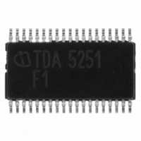
TDA5251
Description
TXRX FSK/ASK SGL LP TSSOP-38
Manufacturer
Infineon Technologies
Type
Transceiverr
Specifications of TDA5251
Package / Case
38-TSSOP
Frequency
315MHz
Data Rate - Maximum
64kbps
Modulation Or Protocol
ASK, FSK
Applications
RKE, Remote Control Systems
Power - Output
13dBm
Sensitivity
-109dBm
Voltage - Supply
2.1 V ~ 5.5 V
Current - Receiving
9.3mA
Current - Transmitting
14mA
Data Interface
PCB, Surface Mount
Antenna Connector
PCB, Surface Mount
Operating Temperature
-40°C ~ 85°C
Operating Frequency
0.35 MHz
Operating Supply Voltage
2.5 V, 3.3 V, 5 V
Maximum Operating Temperature
+ 85 C
Minimum Operating Temperature
- 40 C
Mounting Style
SMD/SMT
Operating Temperature (min)
-40C
Operating Temperature (max)
85C
Operating Temperature Classification
Industrial
Product Depth (mm)
4.4mm
Product Length (mm)
9.7mm
Operating Supply Voltage (min)
2.1V
Operating Supply Voltage (max)
5.5V
Lead Free Status / RoHS Status
Lead free / RoHS Compliant
Memory Size
-
Lead Free Status / Rohs Status
Compliant
Other names
SP000014554
TDA5251
TDA5251INTR
TDA5251XT
TDA5251
TDA5251INTR
TDA5251XT
Available stocks
Company
Part Number
Manufacturer
Quantity
Price
Company:

Part Number:
TDA5251
Manufacturer:
INFINEON
Quantity:
276


Table 2-7
Bus Data Format in I
Table 2-8
Table 2-9
Table 2-10
Table 2-10
* mandatory HIGH
3-wire Bus Mode
In this mode pin 2 (BusMode)= HIGH and Pin 16 (BusData) is in the data input/output pin. Pin 24
(EN) is used to activate the bus interface to allow the transfer of data to / from the device. When pin
24 (EN) is inactive (HIGH), data transfer is inhibited.
Data Transition:
Data transition on pin 16 (BusData) can only occur if the clock BusCLK is LOW. To perform a data
transfer the interface has to be enabled. This is done by setting the EN line to LOW. A serial transfer
is done via BusData, BusCLK and EN. The bit stream needs no chip address.
Data Transfer Write Mode:
To start the communication the EN line has to be set to LOW. The desired sub address byte and
data bytes have to follow. The subaddress (00H...0FH) determines which of the data bytes are
transmitted. At the end of data transition the EN must be HIGH.
Data transfer Read Mode:
To start the communication in the read mode, the EN line has to be set to LOW followed by the sub
address to read (80H, 81H). Afterwards the device is ready to read out data. At the end of data
transition EN must be HIGH.
Data Sheet
STA
STA
STA
MSB
MSB CHIP ADDRESS (WRITE) LSB
MSB CHIP ADDRESS (WRITE) LSB
R7
MSB
1
1
MSB
1
1
1
1
1
1
1
1
CHIP ADDRESS
1
1
1
0
R6
(WRITE)
Chip address Organization
0
I
I
I
I
0
2
2
2
2
0
C Bus Write Mode 8 Bit
C Bus Write Mode 16 Bit
C Bus Read Mode
C Bus Read Mode (continued)
0
0
1
1
0
0
0
0
0
R5
0
2
0
0
0
C Mode
LSB
0
0
ACK S7
DATA OUT FROM SUB ADDRESS
ACK S7
ACK
0
0
MSB
R4
MSB
MSB
S6
S7
0
0
SUB ADDRESS (READ)
S6
S5
S6
00H...08H, 0DH, 0EH, 0FH
SUB ADDRESS (WRITE)
00H...08H, 0DH, 0EH, 0FH
SUB ADDRESS (WRITE)
S5
80H, 81H
S4
S5
R3
0
0
S4
S3
S4
25
S3
S2
S3
LSB
0
1
S2
S1
R2
S2
LSB
S0 ACK STA
S1
S1
LSB
LSB
S0 ACK D15 ... D8 ACK D7 D6 ...
S0 ACK D7
R1
MSB
MSB
MSB
1
Chip Address Write
Chip Address Read
Functional Description
D6 D5 D4 D3 D2 D1 D0 ACK STO
1
CHIP ADDRESS (READ)
R0
LSB
Function
1
DATA IN
0
DATA IN
0
ACK*
TDA5251 F1
Version 1.1
0
0
LSB
2007-02-26
D0
LSB
LSB
1
ACK STO
STO
ACK
Related parts for TDA5251
Image
Part Number
Description
Manufacturer
Datasheet
Request
R

Part Number:
Description:
Manufacturer:
Infineon Technologies AG
Datasheet:
Part Number:
Description:
Manufacturer:
Infineon Technologies AG
Datasheet:
Part Number:
Description:
Manufacturer:
Infineon Technologies AG
Datasheet:
Part Number:
Description:
Manufacturer:
Infineon Technologies AG
Datasheet:
Part Number:
Description:
Manufacturer:
Infineon Technologies AG
Datasheet:
Part Number:
Description:
Manufacturer:
Infineon Technologies AG
Datasheet:
Part Number:
Description:
Manufacturer:
Infineon Technologies AG
Datasheet:
Part Number:
Description:
16-bit microcontroller with 2x2 KByte RAM
Manufacturer:
Infineon Technologies AG
Datasheet:
Part Number:
Description:
NPN silicon RF transistor
Manufacturer:
Infineon Technologies AG
Datasheet:
Part Number:
Description:
NPN silicon RF transistor
Manufacturer:
Infineon Technologies AG
Datasheet:
Part Number:
Description:
NPN silicon RF transistor
Manufacturer:
Infineon Technologies AG
Datasheet:
Part Number:
Description:
NPN silicon RF transistor
Manufacturer:
Infineon Technologies AG
Datasheet:
Part Number:
Description:
Si-MMIC-amplifier in SIEGET 25-technologie
Manufacturer:
Infineon Technologies AG
Datasheet:
Part Number:
Description:
IGBT Power Module
Manufacturer:
Infineon Technologies AG
Datasheet:
Part Number:
Description:
IC for switching-mode power supplies
Manufacturer:
Infineon Technologies AG
Datasheet: