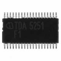
TDA5251 Infineon Technologies, TDA5251 Datasheet - Page 31

TDA5251
Manufacturer Part Number
TDA5251
Description
TXRX FSK/ASK SGL LP TSSOP-38
Manufacturer
Infineon Technologies
Type
Transceiverr
Specifications of TDA5251
Package / Case
38-TSSOP
Frequency
315MHz
Data Rate - Maximum
64kbps
Modulation Or Protocol
ASK, FSK
Applications
RKE, Remote Control Systems
Power - Output
13dBm
Sensitivity
-109dBm
Voltage - Supply
2.1 V ~ 5.5 V
Current - Receiving
9.3mA
Current - Transmitting
14mA
Data Interface
PCB, Surface Mount
Antenna Connector
PCB, Surface Mount
Operating Temperature
-40°C ~ 85°C
Operating Frequency
0.35 MHz
Operating Supply Voltage
2.5 V, 3.3 V, 5 V
Maximum Operating Temperature
+ 85 C
Minimum Operating Temperature
- 40 C
Mounting Style
SMD/SMT
Operating Temperature (min)
-40C
Operating Temperature (max)
85C
Operating Temperature Classification
Industrial
Product Depth (mm)
4.4mm
Product Length (mm)
9.7mm
Operating Supply Voltage (min)
2.1V
Operating Supply Voltage (max)
5.5V
Lead Free Status / RoHS Status
Lead free / RoHS Compliant
Memory Size
-
Lead Free Status / Rohs Status
Compliant
Other names
SP000014554
TDA5251
TDA5251INTR
TDA5251XT
TDA5251
TDA5251INTR
TDA5251XT
Available stocks
Company
Part Number
Manufacturer
Quantity
Price
Company:
Part Number:
TDA5251
Manufacturer:
INFINEON
Quantity:
276
Note: The time delay between start of ON time and the 15µs LOW impulse is 2.6ms + 3 period of
data rate.
If ADC & Data Detect Logic are in continuous mode the 15µs LOW impulse is applied at PwdDD
after each data valid decision.
In self polling mode if D9=0 (Register 00h) and when PwdDD pin level is HIGH the CLK output is
on during ON time and off during OFF time. If D9=1, the CLK output is always on.
TIMER MODE: Only the internal Timer (determined by the ON_TIME and OFF_TIME registers) is
active to support an external logic with periodical Interrupts. After ON_TIME + OFF_TIME a 15µs
LOW impulse is applied at the PwdDD pin (Pin 27).
Figure 2-11
2.4.17
Data signals generate a typical spectrum and this can be used to determine if valid data is on air.
Figure 2-12
The “data valid” criterion is generated from the result of RSSI-TH3 comparison and t
TH1 and TH2 result as shown below. In case of Manchester coding the 0,5*TH1 and 0,5*TH2 gives
improved performance.
The use of permanent data valid recognition makes it absolutely necessary to set the RSSI-ADC
and the Window counter into continuous mode (Register 00H, Bit D5 = D6 = 1).
Data Sheet
TIMER MODE
PwdDD pin in
Data Valid Detection, Data Pin
Timing for Timer Mode
Frequency and RSSI Window
Action
RSSI
Amplitude
15µs
Register 04H
ON_TIME
f
Register 05H
OFF_TIME
Frequency & RSSI Window
31
DATA on air
no DATA on air
15µs
Register 04H
ON_TIME
Frequency
Functional Description
t
t
TDA5251 F1
Version 1.1
timing_timermode.wmf
GATE
data_rate_detect.wmf
2007-02-26
between


