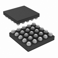
LP3907QTLX-VXSS/NOPB National Semiconductor, LP3907QTLX-VXSS/NOPB Datasheet - Page 10

LP3907QTLX-VXSS/NOPB
Manufacturer Part Number
LP3907QTLX-VXSS/NOPB
Description
IC REG BUCK SYNC-2 LDO-2 25MSMD
Manufacturer
National Semiconductor
Series
PowerWise®r
Datasheet
1.LP3907SQ-JXQXNOPB.pdf
(46 pages)
Specifications of LP3907QTLX-VXSS/NOPB
Topology
Step-Down (Buck) Synchronous (2), Linear (LDO) (2)
Function
Any Function
Number Of Outputs
4
Frequency - Switching
2.1MHz
Voltage/current - Output 1
1.8V, 1A
Voltage/current - Output 2
3.3V, 600mA
Voltage/current - Output 3
2.8V, 300mA
W/led Driver
No
W/supervisor
No
W/sequencer
Yes
Voltage - Supply
2.8 V ~ 5.5 V
Operating Temperature
-40°C ~ 85°C
Mounting Type
Surface Mount
Package / Case
25-UFBGA
Lead Free Status / RoHS Status
Lead free / RoHS Compliant
www.national.com
V
V
ΔV
I
V
PSRR
θn
I
Note
T
C
V
V
Eff
I
f
I
I
R
R
T
C
C
SC
Q
SHDN
OSC
PEAK
Q
ON
ON
IN
OUT
IN
FB
OUT
OUT
DSON
DSON
IN
O
Low Drop Out Regulators, LDO1 and LDO2
Unless otherwise noted, V
25°C. Limits appearing in boldface type apply over the entire junction temperature range for operation, −40°C to +125°C.
2,
Buck Converters SW1, SW2
Unless otherwise noted, V
type apply for T
C to +125°C.
(Note
(Note
OUT
Symbol
Symbol
– V
Note
14)
Accuracy Output Voltage Accuracy (Default V
(P)
(N)
OUT
14)
11,
7,
Note
(Note
Feedback Voltage
Line Regulation
Load Regulation
Efficiency
Shutdown Supply Current
Internal Oscillator Frequency
Buck1 Peak Switching Current Limit
Buck2 Peak Switching Current Limit
Quiescent Current “On”
Pin-Pin Resistance PFET
Pin-Pin Resistance NFET
Turn On Time
Input Capacitor
Output Capacitor
Operational Voltage Range
Line Regulation
Load Regulation
Short Circuit Current Limit
Dropout Voltage
Power Supply Ripple Rejection
Supply Output Noise
Quiescent Current “On”
Quiescent Current “On”
Quiescent Current “Off”
Turn On Time
Output Capacitor
J
8,
= 25°C. Limits appearing in boldface type apply over the entire junction temperature range for operation, −40°
Note
2,
Note
9,
IN
IN
Note
7,
= 3.6, C
Parameter
= 3.6, C
Parameter
Note
10,
Note
8,
IN
IN
= 10 µF, C
Note
= 1.0µF, C
11,
9,
Note
Note
OUT
OUT
12)
OUT
11,
= 10 µF, L
= 0.47µF. Typical values and limits appearing in normal type apply for T
) Load current = 1 mA
2.8< V
I
100mA < I
Load Current = 250mA
EN is de-asserted
No load PFM Mode
Start up from shut-down
Capacitance for stability
Capacitance for stability
Note
O
VINLDO1 and VINLDO2 PMOS
pins
V
(Note
V
Load Current = 1mA to I
LDO1-2, V
Load Current = 50mA
(Note
F = 10kHz, Load Current = I
10Hz < F < 100KHz
I
I
EN is
Start up from shut-down
Capacitance for stability
0°C
−40°C
ESR
=10mA
OUT
OUT
IN
IN
= (V
= 3.6V,
18)
≤
IN
= 0mA
= I
(Note
OUT
de-asserted(Note
12), Load Current = mA
10)
10
T
< 5.5
≤
MAX
OUT
J
O
T
= 2.2 µH ceramic. Typical values and limits appearing in normal
Conditions
≤
< I
Conditions
J
OUT
15)
125°C
+ 0.3V) to 5.0V,
≤
MAX
125°C
= 0V
MAX
16)
MAX
1.74
0.33
0.68
Min
Min
1.7
−3
10
10
−3
5
0.0013
0.089
0.01
Typ
0.03
0.47
200
180
500
Typ
500
300
2.1
1.5
1.0
1.0
96
33
30
45
80
40
60
0.011
Max
Max
0.15
200
500
+3
5.5
3
(Note
µVrms
%/mA
%/mA
Units
Units
MHz
%/V
%/V
mΩ
mΩ
mΩ
mA
mV
µA
µA
µF
µF
J
dB
µA
µA
µA
µs
µs
µF
µF
%
%
%
A
V
=


