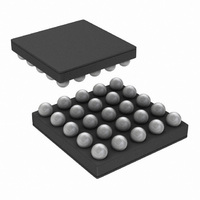
LP3907QTLX-VXSS/NOPB National Semiconductor, LP3907QTLX-VXSS/NOPB Datasheet - Page 37

LP3907QTLX-VXSS/NOPB
Manufacturer Part Number
LP3907QTLX-VXSS/NOPB
Description
IC REG BUCK SYNC-2 LDO-2 25MSMD
Manufacturer
National Semiconductor
Series
PowerWise®r
Datasheet
1.LP3907SQ-JXQXNOPB.pdf
(46 pages)
Specifications of LP3907QTLX-VXSS/NOPB
Topology
Step-Down (Buck) Synchronous (2), Linear (LDO) (2)
Function
Any Function
Number Of Outputs
4
Frequency - Switching
2.1MHz
Voltage/current - Output 1
1.8V, 1A
Voltage/current - Output 2
3.3V, 600mA
Voltage/current - Output 3
2.8V, 300mA
W/led Driver
No
W/supervisor
No
W/sequencer
Yes
Voltage - Supply
2.8 V ~ 5.5 V
Operating Temperature
-40°C ~ 85°C
Mounting Type
Surface Mount
Package / Case
25-UFBGA
Lead Free Status / RoHS Status
Lead free / RoHS Compliant
BUCK FUNCTION REGISTER (BFCR) – 0x38
This register allows the Buck switcher clock frequency to be
spread across a wider range, allowing for less Electro-mag-
This register also allows dynamic scaling of the nPOR Delay
Timing. The LP3907 is equipped with an internal Power-On-
Reset (“POR”) circuit which monitors the output voltage levels
on the buck regulators, allowing the user to more actively
monitor the power status of the chip.
The Under Voltage Lock-Out feature continuously monitor the
raw input supply voltage (VINLDO12) and automatically dis-
ables the four voltage regulators whenever this supply voltage
Name
Access
Data
Reset
Reserved
D7-2
000
—
—
BP_UVLO
R/W
Bypass UVLO
monitoring
0 - Allow UVLO
1 - Disable UVLO
Programmed
Factory-
Default
D4
TPOR
R/w
nPOR Delay Timing
00 - 50µs
01 - 50ms
10 - 100ms
11 - 200ms
D3
01
37
netic Interference (EMI). The spread spectrum modulation
frequency refers to the rate at which the frequency ramps up
and down, centered at 2MHz.
is less than 2.8VDC. This prevents the user from damaging
the power source (i.e. battery), but can be disabled if the user
wishes.
Note that if the supply to VDD_M is close to 2.8V with a heavy
load current on the regulators, the chip is in danger of pow-
ering down due to UVLO. If the user wishes to keep the chip
active under those conditions, enable the “Bypass UVLO”
feature.
BK_SLOMOD
R/W
Buck Spread Spectrum
Modulation
0 – 10 kHz triangular wave
1 – 2 kHz triangular wave
D1
1
BK_SSEN
R/W
Spread Spectrum
Function Output
0 – Disabled
1 – Enabled
D0
0
30017825
www.national.com


