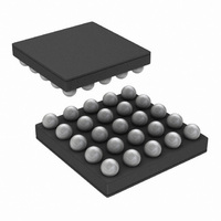
LP3907QTLX-VXSS/NOPB National Semiconductor, LP3907QTLX-VXSS/NOPB Datasheet - Page 19

LP3907QTLX-VXSS/NOPB
Manufacturer Part Number
LP3907QTLX-VXSS/NOPB
Description
IC REG BUCK SYNC-2 LDO-2 25MSMD
Manufacturer
National Semiconductor
Series
PowerWise®r
Datasheet
1.LP3907SQ-JXQXNOPB.pdf
(46 pages)
Specifications of LP3907QTLX-VXSS/NOPB
Topology
Step-Down (Buck) Synchronous (2), Linear (LDO) (2)
Function
Any Function
Number Of Outputs
4
Frequency - Switching
2.1MHz
Voltage/current - Output 1
1.8V, 1A
Voltage/current - Output 2
3.3V, 600mA
Voltage/current - Output 3
2.8V, 300mA
W/led Driver
No
W/supervisor
No
W/sequencer
Yes
Voltage - Supply
2.8 V ~ 5.5 V
Operating Temperature
-40°C ~ 85°C
Mounting Type
Surface Mount
Package / Case
25-UFBGA
Lead Free Status / RoHS Status
Lead free / RoHS Compliant
DC/DC Converters
OVERVIEW
The LP3907 supplies the various power needs of the appli-
cation by means of two Linear Low Drop Regulators (LDO1
*For default values of the regulators, please consult page 3 of this datasheet.
LINEAR LOW DROPOUT REGULATORS (LDOS)
LDO1 and LDO2 are identical linear regulators targeting ana-
log loads characterized by low noise requirements. LDO1 and
LDO2 are enabled through the ENLDO pin or through the
corresponding LDO1 or LDO2 control register. The output
NO-LOAD STABILITY
The LDOs will remain stable and in regulation with no external
load. This is an important consideration in some circuits, for
example, CMOS RAM keep-alive applications.
LDO1 AND LDO2 CONTROL REGISTERS
LDO1 and LDO2 can be configured by means of the LDO1
and LDO2 control registers. The output voltage is pro-
Supply
LDO1
LDO2
SW1
SW2
analog
analog
digital
digital
Load
V
OUT
1.0 to 3.5
1.0 to 3.5
0.8 to 2.0
1.0 to 3.5
Supply Specification
Range(V)
19
and LDO2) and two Buck converters (SW1 and SW2). The
table hereunder lists the output characteristics of the various
regulators.
voltages of both LDOs are register programmable. The de-
fault output voltages are factory programmed during Final
Test, which can be tailored to the specific needs of the system
designer.
grammable in steps of 100mV from 1.0V to 3.5V by program-
ming bits D4-0 in the LDO Control registers. Both LDO1 and
LDO2 are enabled by applying a logic 1 to the ENLDO1 and
ENLDO2 pin. Enable/disable control is also provided through
enable bit of the LDO1 and LDO2 control registers. The value
of the enable LDO bit in the register is logic 1 by default. The
output voltage can be altered while the LDO is enabled.
Resolution (mV)
100
100
100
50
Output
30017822
Maximum Output
Current (mA)
1000
I
300
300
600
MAX
www.national.com


