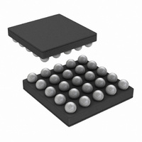
LP3907QTLX-VXSS/NOPB National Semiconductor, LP3907QTLX-VXSS/NOPB Datasheet - Page 42

LP3907QTLX-VXSS/NOPB
Manufacturer Part Number
LP3907QTLX-VXSS/NOPB
Description
IC REG BUCK SYNC-2 LDO-2 25MSMD
Manufacturer
National Semiconductor
Series
PowerWise®r
Datasheet
1.LP3907SQ-JXQXNOPB.pdf
(46 pages)
Specifications of LP3907QTLX-VXSS/NOPB
Topology
Step-Down (Buck) Synchronous (2), Linear (LDO) (2)
Function
Any Function
Number Of Outputs
4
Frequency - Switching
2.1MHz
Voltage/current - Output 1
1.8V, 1A
Voltage/current - Output 2
3.3V, 600mA
Voltage/current - Output 3
2.8V, 300mA
W/led Driver
No
W/supervisor
No
W/sequencer
Yes
Voltage - Supply
2.8 V ~ 5.5 V
Operating Temperature
-40°C ~ 85°C
Mounting Type
Surface Mount
Package / Case
25-UFBGA
Lead Free Status / RoHS Status
Lead free / RoHS Compliant
www.national.com
Thermal Performance of the LLP
Package
The LP3907 is a monolithic device with integrated power
FETs. For that reason, it is important to pay special attention
to the thermal impedance of the LLP package and to the PCB
layout rules in order to maximize power dissipation of the LLP
package.
The LLP package is designed for enhanced thermal perfor-
mance and features an exposed die attach pad at the bottom
center of the package that creates a direct path to the PCB
for maximum power dissipation. Compared to the traditional
leaded packages where the die attach pad is embedded in-
side the molding compound, the LLP reduces one layer in the
thermal path.
The thermal advantage of the LLP package is fully realized
only when the exposed die attach pad is soldered down to a
thermal land on the PCB board with thermal vias planted un-
42
derneath the thermal land. Based on thermal analysis of the
LLP package, the junction-to-ambient thermal resistance
(θJA) can be improved by a factor of two when the die attach
pad of the LLP package is soldered directly onto the PCB with
thermal land and thermal vias, as opposed to an alternative
with no direct soldering to a thermal land. Typical pitch and
outer diameter for thermal vias are 1.27mm and 0.33mm re-
spectively. Typical copper via barrel plating is 1oz, although
thicker copper may be used to further improve thermal per-
formance. The LP3907 die attach pad is connected to the
substrate of the IC and therefore, the thermal land and vias
on the PCB board need to be connected to ground (GND pin).
For more information on board layout techniques, refer to Ap-
plication Note AN–1187 “Leadless Lead frame Package
(LLP).” on http://www.national.com This application note also
discusses package handling, solder stencil and the assembly
process.


