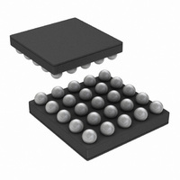
LP3907QTLX-VXSS/NOPB National Semiconductor, LP3907QTLX-VXSS/NOPB Datasheet - Page 26

LP3907QTLX-VXSS/NOPB
Manufacturer Part Number
LP3907QTLX-VXSS/NOPB
Description
IC REG BUCK SYNC-2 LDO-2 25MSMD
Manufacturer
National Semiconductor
Series
PowerWise®r
Datasheet
1.LP3907SQ-JXQXNOPB.pdf
(46 pages)
Specifications of LP3907QTLX-VXSS/NOPB
Topology
Step-Down (Buck) Synchronous (2), Linear (LDO) (2)
Function
Any Function
Number Of Outputs
4
Frequency - Switching
2.1MHz
Voltage/current - Output 1
1.8V, 1A
Voltage/current - Output 2
3.3V, 600mA
Voltage/current - Output 3
2.8V, 300mA
W/led Driver
No
W/supervisor
No
W/sequencer
Yes
Voltage - Supply
2.8 V ~ 5.5 V
Operating Temperature
-40°C ~ 85°C
Mounting Type
Surface Mount
Package / Case
25-UFBGA
Lead Free Status / RoHS Status
Lead free / RoHS Compliant
www.national.com
The above timing diagram details the Power good with delay
with respect to the enable signals EN1, and EN2. The RDY1,
RDY2 are internal signals derived from the output of two com-
parators. Each comparator has been trimmed as follows:
The circuits for EN1 and RDY1 is symmetrical to EN2 and
RDY2, so each reference to EN1 and RDY1 will also work for
EN2 and RDY2 and vice versa.
Comparator Level
HIGH
LOW
Buck Supply Level
Greater than 94%
Less than 85%
Faults Occurring in Counter Delay After Startup
26
If EN1 and RDY1 signals are High at time t1, then the RDY1
signal rising edge triggers the programmable delay counter
(50μs, 50ms, 100ms, 200ms). This delay forces nPOR LOW
between time interval t1 and t2. nPOR is then pulled high after
the programmable delay is completed. Now if EN2 and RDY2
are initiated during this interval the nPOR signal ignores this
event.
If either RDY1or RDY2 were to go LOW at t3 then the pro-
grammable delay is triggered again.
30017881


