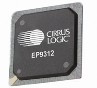
EP9312-CB Cirrus Logic Inc, EP9312-CB Datasheet - Page 497

EP9312-CB
Manufacturer Part Number
EP9312-CB
Description
System-on-Chip Processor
Manufacturer
Cirrus Logic Inc
Series
EP9r
Datasheets
1.EP9307-CRZ.pdf
(824 pages)
2.EP9312-IBZ.pdf
(4 pages)
3.EP9312-CB.pdf
(62 pages)
4.EP9312-CB.pdf
(17 pages)
Specifications of EP9312-CB
Peak Reflow Compatible (260 C)
No
A/d Converter
12 Bits
Leaded Process Compatible
No
No. Of I/o Pins
65
Package / Case
352-BGA
Core Processor
ARM9
Core Size
16/32-Bit
Speed
200MHz
Connectivity
EBI/EMI, EIDE, Ethernet, I²C, IrDA, Keypad/Touchscreen, SPI, UART/USART, USB
Peripherals
AC'97, DMA, I²:S, LCD, LED, MaverickKey, POR, PWM, WDT
Number Of I /o
16
Program Memory Type
ROMless
Ram Size
32K x 8
Voltage - Supply (vcc/vdd)
1.65 V ~ 3.6 V
Data Converters
A/D 8x12b
Oscillator Type
External
Operating Temperature
0°C ~ 70°C
Processor Series
EP93xx
Core
ARM920T
Data Bus Width
32 bit
3rd Party Development Tools
MDK-ARM, RL-ARM, ULINK2
Lead Free Status / RoHS Status
Contains lead / RoHS non-compliant
Eeprom Size
-
Program Memory Size
-
Lead Free Status / Rohs Status
No
Other names
598-1257
Available stocks
Company
Part Number
Manufacturer
Quantity
Price
Part Number:
EP9312-CB
Manufacturer:
CIRRUS
Quantity:
20 000
- EP9307-CRZ PDF datasheet
- EP9312-IBZ PDF datasheet #2
- EP9312-CB PDF datasheet #3
- EP9312-CB PDF datasheet #4
- Current page: 497 of 824
- Download datasheet (13Mb)
DS785UM1
13.1 Introduction
13.2 Booting from SyncROM or SyncFLASH
The SDRAM controller provides a high speed memory interface to single-data-rate SDRAMs,
Synchronous FLASH, and Synchronous ROMs.
The key features of the SDRAM controller are:
During power-on reset, if the values on the processor pins shown in
either a Synchronous ROM device or Synchronous FLASH device to be used for booting up
the processor, a short configuration sequence is activated and completed before the
processor is released from power-on reset. By default, Synchronous Memory Bank 3,
controlled by device configuration register SDRAMDevCfg[3:0], is used for booting.
For a Synchronous ROM device, the configuration sequence writes RAS = 0x2 and CAS =
0x5 to the SDRAMDevCfg[3:0] register and writes RAS = 0x2, CAS = 0x5, and either Burst
Note: In the EP9301 and 9302 processors, the common address/data bus is 16-bits wide
Note: In the EP9307, EP9312, and EP9315 processors, the common address/data bus is
• Raster DMA input port for high-bandwidth display refreshing.
• Up to four synchronous memory banks that can be independently configured
• Special configuration bits for Synchronous ROM operation
• Ability to program Synchronous FLASH devices using write and erase commands
• Data is transferred between the controller and the synchronous memory device in quad-
• Programmable for 16 or 32-bit data bus: EP9307, EP9312, and EP9315 processors only
• SDRAM contents are preserved when a “soft” reset is asserted
• Power saving synchronous memory clock enable
word bursts.
13SDRAM, SyncROM, and SyncFLASH Controller
and the SDRAM, SyncROM, and SyncFLASH synchronous memory controller
supports 16-bit and 8-bit devices.
programmable to be either 16-bits or 32-bits wide and the SDRAM, SyncROM, and
SyncFLASH synchronous memory controller supports 32-bit , 16-bit, and 8-bit
devices.
Copyright 2007 Cirrus Logic
Table CAUTION:
Chapter 13
select
13-1
13
Related parts for EP9312-CB
Image
Part Number
Description
Manufacturer
Datasheet
Request
R

Part Number:
Description:
IC ARM920T MCU 200MHZ 352-PBGA
Manufacturer:
Cirrus Logic Inc
Datasheet:

Part Number:
Description:
IC ARM9 SOC UNIVERSAL 352PBGA
Manufacturer:
Cirrus Logic Inc
Datasheet:

Part Number:
Description:
IC ARM920T MCU 200MHZ 352-PBGA
Manufacturer:
Cirrus Logic Inc
Datasheet:

Part Number:
Description:
IC Universal Platform ARM9 SOC Prcessor
Manufacturer:
Cirrus Logic Inc
Datasheet:

Part Number:
Description:
IC Universal Platform ARM9 SOC Prcessor
Manufacturer:
Cirrus Logic Inc
Datasheet:

Part Number:
Description:
Development Kit
Manufacturer:
Cirrus Logic Inc
Datasheet:

Part Number:
Description:
Development Kit
Manufacturer:
Cirrus Logic Inc
Datasheet:

Part Number:
Description:
High-efficiency PFC + Fluorescent Lamp Driver Reference Design
Manufacturer:
Cirrus Logic Inc
Datasheet:

Part Number:
Description:
Development Kit
Manufacturer:
Cirrus Logic Inc
Datasheet:

Part Number:
Description:
Development Kit
Manufacturer:
Cirrus Logic Inc
Datasheet:

Part Number:
Description:
Development Kit
Manufacturer:
Cirrus Logic Inc
Datasheet:

Part Number:
Description:
Development Kit
Manufacturer:
Cirrus Logic Inc
Datasheet:

Part Number:
Description:
Ref Bd For Speakerbar MSA & DSP Products
Manufacturer:
Cirrus Logic Inc


