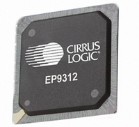
EP9312-CB Cirrus Logic Inc, EP9312-CB Datasheet - Page 664

EP9312-CB
Manufacturer Part Number
EP9312-CB
Description
System-on-Chip Processor
Manufacturer
Cirrus Logic Inc
Series
EP9r
Datasheets
1.EP9307-CRZ.pdf
(824 pages)
2.EP9312-IBZ.pdf
(4 pages)
3.EP9312-CB.pdf
(62 pages)
4.EP9312-CB.pdf
(17 pages)
Specifications of EP9312-CB
Peak Reflow Compatible (260 C)
No
A/d Converter
12 Bits
Leaded Process Compatible
No
No. Of I/o Pins
65
Package / Case
352-BGA
Core Processor
ARM9
Core Size
16/32-Bit
Speed
200MHz
Connectivity
EBI/EMI, EIDE, Ethernet, I²C, IrDA, Keypad/Touchscreen, SPI, UART/USART, USB
Peripherals
AC'97, DMA, I²:S, LCD, LED, MaverickKey, POR, PWM, WDT
Number Of I /o
16
Program Memory Type
ROMless
Ram Size
32K x 8
Voltage - Supply (vcc/vdd)
1.65 V ~ 3.6 V
Data Converters
A/D 8x12b
Oscillator Type
External
Operating Temperature
0°C ~ 70°C
Processor Series
EP93xx
Core
ARM920T
Data Bus Width
32 bit
3rd Party Development Tools
MDK-ARM, RL-ARM, ULINK2
Lead Free Status / RoHS Status
Contains lead / RoHS non-compliant
Eeprom Size
-
Program Memory Size
-
Lead Free Status / Rohs Status
No
Other names
598-1257
Available stocks
Company
Part Number
Manufacturer
Quantity
Price
Part Number:
EP9312-CB
Manufacturer:
CIRRUS
Quantity:
20 000
- EP9307-CRZ PDF datasheet
- EP9312-IBZ PDF datasheet #2
- EP9312-CB PDF datasheet #3
- EP9312-CB PDF datasheet #4
- Current page: 664 of 824
- Download datasheet (13Mb)
21
21-8
I
EP93xx User’s Guide
2
S Controller
order to generate a set of audio clocks, LRCK (word clock) and SCLK (bit clock). The control
bits required are:
These control bits come from the TX and the RX clock configuration registers and the word
length registers. This control is sent out through the i2s_mstr_clk_cfg port of the I
to the audio clock generator. The audio clock generator responds with the correct clock
definition based on the settings received.
If both the TX and RX are required to be in master mode at the same time, both the RX and
TX share the same master audio clocks. The following shows how i2s_mstr_clk_cfg is
generated.
Please note, the I2SClkDiv (Addr=0x8093_008C) register in the SYSCON block has an effect
on I
for each function is determined by the ORIDE bit in the I2SClkDiv register (I2SClkDiv[29]).
This table does not show the details of how to control this function. Please refer to each
individual block for a detailed description.
• Master Mode Enable. (i2s_mstr_clk_cfg[0])
• Word Length Control (i2s_mstr_clk_cfg[2:1])
• Bit Clock Polarity (i2s_mstr_clk_cfg[3])
• Not Bit Clock Gating (i2s_mstr_clk_cfg[4]).
• Bit Clock Rate (i2s_mstr_clk_cfg[6:5])
• If the Transmitter is enabled, the clock configuration information will always come from
• If the Transmitter is disabled and the Receiver is required to be in master mode, then the
2
I2STXClkCfg register. Therefore, the I2SRXClkCfg (receiver clock configuration) register
must be configured to be the same as the I2STXClkCfg (transmitter clock configuration)
register in order to ensure correct operation of the receiver. The word lengths for both
the TX and RX must be the same.
i2s_mstr_clk_cfg output is generated from the I2SRXClkCfg register and the RX word
length register.
S clock generation as well. The details are listed in
SCLK polarity
SCLK Speed and
Gating
LRCK Speed
Audio Slave Mode
Audio Clock
(SCLK, LRCLK)
Generation Enable
Function
Table 21-4. I2SClkDiv SYSCON Register Effect on I
SPOL (I2SClkDiv[19])
DROP(I2SClkDiv[20]),
SDIV(I2SClkDiv[16])
LRDIV(I2SClkDiv[18:17])
SLAVE(I2SClkDiv[30])
SENA(I2SClkDiv[31])
Copyright 2007 Cirrus Logic
ORIDE=1
Table
i2s_mstr_clk_cfg[3]
SCLK always is MCLK/2.
SCLK is gated when
i2s_mstr_clk_cfg[4]=0,
i2s_mstr_clk_cfg[6:5]=0 and
i2s_mstr_clk_cfg[2:1]=1, otherwise,
SCLK is not gated.
i2s_mstr_clk_cfg[6:5]
i2s_mstr_clk_cfg[0]
I2SonAC97 (DeviceCfg[6]) or
I2SonSSP (DeviceCfg[7]). If either
one is set, it enables the clock
generation.
2
S Clock Generation
21-4. The controlling bit field
ORIDE=0
2
S controller
DS785UM1
Related parts for EP9312-CB
Image
Part Number
Description
Manufacturer
Datasheet
Request
R

Part Number:
Description:
IC ARM920T MCU 200MHZ 352-PBGA
Manufacturer:
Cirrus Logic Inc
Datasheet:

Part Number:
Description:
IC ARM9 SOC UNIVERSAL 352PBGA
Manufacturer:
Cirrus Logic Inc
Datasheet:

Part Number:
Description:
IC ARM920T MCU 200MHZ 352-PBGA
Manufacturer:
Cirrus Logic Inc
Datasheet:

Part Number:
Description:
IC Universal Platform ARM9 SOC Prcessor
Manufacturer:
Cirrus Logic Inc
Datasheet:

Part Number:
Description:
IC Universal Platform ARM9 SOC Prcessor
Manufacturer:
Cirrus Logic Inc
Datasheet:

Part Number:
Description:
Development Kit
Manufacturer:
Cirrus Logic Inc
Datasheet:

Part Number:
Description:
Development Kit
Manufacturer:
Cirrus Logic Inc
Datasheet:

Part Number:
Description:
High-efficiency PFC + Fluorescent Lamp Driver Reference Design
Manufacturer:
Cirrus Logic Inc
Datasheet:

Part Number:
Description:
Development Kit
Manufacturer:
Cirrus Logic Inc
Datasheet:

Part Number:
Description:
Development Kit
Manufacturer:
Cirrus Logic Inc
Datasheet:

Part Number:
Description:
Development Kit
Manufacturer:
Cirrus Logic Inc
Datasheet:

Part Number:
Description:
Development Kit
Manufacturer:
Cirrus Logic Inc
Datasheet:

Part Number:
Description:
Ref Bd For Speakerbar MSA & DSP Products
Manufacturer:
Cirrus Logic Inc


