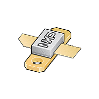
BLF871 NXP Semiconductors, BLF871 Datasheet - Page 8

BLF871
Manufacturer Part Number
BLF871
Description
LDMOS,RF,100W,UHF,50V
Manufacturer
NXP Semiconductors
Datasheet
1.BLF871112.pdf
(19 pages)
Specifications of BLF871
Drain Source Voltage Vds
89V
Continuous Drain Current Id
3.7A
Operating Frequency Range
108MHz To 225MHz
Rf Transistor Case
SOT-467C
No. Of Pins
2
Transistor Type
RF MOSFET
Application
UHF
Channel Type
N
Channel Mode
Enhancement
Drain Source Voltage (max)
89V
Output Power (max)
100W(Typ)
Power Gain (typ)@vds
21@40V/21@40V/22@40VdB
Frequency (max)
860MHz
Package Type
LDMOST
Pin Count
3
Drain Source Resistance (max)
210(Typ)@6.15Vmohm
Input Capacitance (typ)@vds
95@40VpF
Output Capacitance (typ)@vds
30@40VpF
Reverse Capacitance (typ)
1@40VpF
Operating Temp Range
-65C to 200C
Drain Efficiency (typ)
60%
Mounting
Screw
Mode Of Operation
2-Tone Class-AB/CW Class-AB/DVB-T
Number Of Elements
1
Vswr (max)
10
Screening Level
Military
Lead Free Status / RoHS Status
Lead free / RoHS Compliant
Available stocks
Company
Part Number
Manufacturer
Quantity
Price
Company:
Part Number:
BLF871
Manufacturer:
ROHM
Quantity:
12 000
Company:
Part Number:
BLF871,112
Manufacturer:
UMS
Quantity:
1 400
Company:
Part Number:
BLF871S
Manufacturer:
TOSHIBA
Quantity:
5 000
Company:
Part Number:
BLF871S112
Manufacturer:
NXP Semiconductors
Quantity:
135
NXP Semiconductors
BLF871_BLF871S_4
Product data sheet
Fig 9.
Fig 11. DVB-T PAR at 0.1 % and at 0.01 % probability on the CCDF as function of frequency; typical values
(dB)
G
(1) V
(2) V
(1) PAR at 0.01 % probability on the CCDF; V
(2) PAR at 0.01 % probability on the CCDF; V
(3) PAR at 0.1 % probability on the CCDF; V
(4) PAR at 0.1 % probability on the CCDF; V
p
22
20
18
16
400
I
test circuit as described in
DVB-T power gain and drain efficiency as
functions of frequency; typical values
I
PAR of input signal = 9.5 dB at 0.01 % probability on CCDF.
Dq
Dq
DS
DS
= 0.5 A; measured in a common source broadband
= 0.5 A; measured in a common source broadband test circuit as described in
= 40 V; P
= 42 V; P
7.2.2 DVB-T
500
G
η
D
p
L(AV)
L(AV)
600
= 22 W
= 24 W
700
Section
(2)
(1)
(1)
(2)
PAR
(dB)
9
8
7
6
5
400
8.
800
001aaj284
f (MHz)
DS
DS
DS
DS
Rev. 04 — 19 November 2009
500
= 40 V; P
= 42 V; P
900
= 40 V; P
= 42 V; P
50
40
30
20
(%)
η
D
600
L(AV)
L(AV)
L(AV)
L(AV)
= 22 W
= 24 W
= 22 W
= 24 W
Fig 10. DVB-T third order intermodulation distortion
700
IMD3
(dBc)
(1)
(2)
(3)
(4)
(1) V
(2) V
−20
−40
−60
0
400
I
test circuit as described in
as a function of frequency; typical values
800
Dq
DS
DS
001aaj286
f (MHz)
= 0.5 A; measured in a common source broadband
= 40 V; P
= 42 V; P
500
900
BLF871; BLF871S
Section
L(AV)
L(AV)
600
UHF power LDMOS transistor
= 22 W
= 24 W
8.
700
Section
(2)
(1)
8.
© NXP B.V. 2010. All rights reserved.
800
001aaj285
f (MHz)
900
8 of 19


