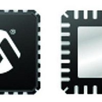
DSPIC33FJ32GP204-H/ML Microchip Technology, DSPIC33FJ32GP204-H/ML Datasheet - Page 193

DSPIC33FJ32GP204-H/ML
Manufacturer Part Number
DSPIC33FJ32GP204-H/ML
Description
16-bit DSC, 44LD,32KB Flash,40 MIPS,nanoWatt 44 QFN 8x8x0.9mm TUBE
Manufacturer
Microchip Technology
Series
dsPIC™ 33Fr
Datasheet
1.DSPIC33FJ16GP304-IPT.pdf
(284 pages)
Specifications of DSPIC33FJ32GP204-H/ML
Core Processor
dsPIC
Core Size
16-Bit
Speed
40 MIPs
Connectivity
I²C, IrDA, LIN, SPI, UART/USART
Peripherals
Brown-out Detect/Reset, POR, PWM, WDT
Number Of I /o
35
Program Memory Size
32KB (32K x 8)
Program Memory Type
FLASH
Ram Size
2K x 8
Voltage - Supply (vcc/vdd)
3 V ~ 3.6 V
Data Converters
A/D 13x12b
Oscillator Type
Internal
Operating Temperature
-40°C ~ 140°C
Package / Case
44-VQFN Exposed Pad
Processor Series
dsPIC33F
Core
dsPIC
Data Bus Width
16 bit
Interface Type
SPI, I2C, UART, JTAG
Number Of Programmable I/os
35
Operating Supply Voltage
3.3 V
Maximum Operating Temperature
+ 140 C
Mounting Style
SMD/SMT
Development Tools By Supplier
MPLAB IDE Software
Minimum Operating Temperature
- 40 C
On-chip Adc
10 bit, 13 Channel
Lead Free Status / RoHS Status
Lead free / RoHS Compliant
Eeprom Size
-
Lead Free Status / Rohs Status
Details
- Current page: 193 of 284
- Download datasheet (4Mb)
TABLE 20-1:
© 2011 Microchip Technology Inc.
Wm*Wm
Wm*Wn
Wn
Wnd
Wns
WREG
Ws
Wso
Wx
Wxd
Wy
Wyd
dsPIC33FJ32GP202/204 and dsPIC33FJ16GP304
Field
SYMBOLS USED IN OPCODE DESCRIPTIONS (CONTINUED)
Multiplicand and Multiplier working register pair for Square instructions ∈
{W4 * W4,W5 * W5,W6 * W6,W7 * W7}
Multiplicand and Multiplier working register pair for DSP instructions ∈
{W4 * W5,W4 * W6,W4 * W7,W5 * W6,W5 * W7,W6 * W7}
One of 16 working registers ∈ {W0..W15}
One of 16 destination working registers ∈ {W0...W15}
One of 16 source working registers ∈ {W0...W15}
W0 (working register used in file register instructions)
Source W register ∈ { Ws, [Ws], [Ws++], [Ws--], [++Ws], [--Ws] }
Source W register ∈
{ Wns, [Wns], [Wns++], [Wns--], [++Wns], [--Wns], [Wns+Wb] }
X data space prefetch address register for DSP instructions
∈ {[W8]+ = 6, [W8]+ = 4, [W8]+ = 2, [W8], [W8]- = 6, [W8]- = 4, [W8]- = 2,
X data space prefetch destination register for DSP instructions ∈ {W4...W7}
Y data space prefetch address register for DSP instructions
∈ {[W10]+ = 6, [W10]+ = 4, [W10]+ = 2, [W10], [W10]- = 6, [W10]- = 4, [W10]- = 2,
Y data space prefetch destination register for DSP instructions ∈ {W4...W7}
[W9]+ = 6, [W9]+ = 4, [W9]+ = 2, [W9], [W9]- = 6, [W9]- = 4, [W9]- = 2,
[W9 + W12], none}
[W11]+ = 6, [W11]+ = 4, [W11]+ = 2, [W11], [W11]- = 6, [W11]- = 4, [W11]- = 2,
[W11 + W12], none}
Description
DS70290G-page 193
Related parts for DSPIC33FJ32GP204-H/ML
Image
Part Number
Description
Manufacturer
Datasheet
Request
R

Part Number:
Description:
IC, DSC, 16BIT, 12KB, 40MHZ, 3.6V, DIP28
Manufacturer:
Microchip Technology
Datasheet:

Part Number:
Description:
Manufacturer:
Microchip Technology Inc.
Datasheet:

Part Number:
Description:
Manufacturer:
Microchip Technology Inc.
Datasheet:

Part Number:
Description:
Manufacturer:
Microchip Technology Inc.
Datasheet:

Part Number:
Description:
Manufacturer:
Microchip Technology Inc.
Datasheet:

Part Number:
Description:
Manufacturer:
Microchip Technology Inc.
Datasheet:

Part Number:
Description:
Manufacturer:
Microchip Technology Inc.
Datasheet:

Part Number:
Description:
Manufacturer:
Microchip Technology Inc.
Datasheet:

Part Number:
Description:
Manufacturer:
Microchip Technology Inc.
Datasheet:


