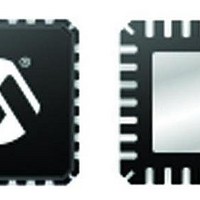
DSPIC33FJ32GP204-H/ML Microchip Technology, DSPIC33FJ32GP204-H/ML Datasheet - Page 57

DSPIC33FJ32GP204-H/ML
Manufacturer Part Number
DSPIC33FJ32GP204-H/ML
Description
16-bit DSC, 44LD,32KB Flash,40 MIPS,nanoWatt 44 QFN 8x8x0.9mm TUBE
Manufacturer
Microchip Technology
Series
dsPIC™ 33Fr
Datasheet
1.DSPIC33FJ16GP304-IPT.pdf
(284 pages)
Specifications of DSPIC33FJ32GP204-H/ML
Core Processor
dsPIC
Core Size
16-Bit
Speed
40 MIPs
Connectivity
I²C, IrDA, LIN, SPI, UART/USART
Peripherals
Brown-out Detect/Reset, POR, PWM, WDT
Number Of I /o
35
Program Memory Size
32KB (32K x 8)
Program Memory Type
FLASH
Ram Size
2K x 8
Voltage - Supply (vcc/vdd)
3 V ~ 3.6 V
Data Converters
A/D 13x12b
Oscillator Type
Internal
Operating Temperature
-40°C ~ 140°C
Package / Case
44-VQFN Exposed Pad
Processor Series
dsPIC33F
Core
dsPIC
Data Bus Width
16 bit
Interface Type
SPI, I2C, UART, JTAG
Number Of Programmable I/os
35
Operating Supply Voltage
3.3 V
Maximum Operating Temperature
+ 140 C
Mounting Style
SMD/SMT
Development Tools By Supplier
MPLAB IDE Software
Minimum Operating Temperature
- 40 C
On-chip Adc
10 bit, 13 Channel
Lead Free Status / RoHS Status
Lead free / RoHS Compliant
Eeprom Size
-
Lead Free Status / Rohs Status
Details
- Current page: 57 of 284
- Download datasheet (4Mb)
5.0
The
dsPIC33FJ16GP304 devices contain internal Flash
program memory for storing and executing application
code. The memory is readable, writable and erasable
during normal operation over the entire V
Flash memory can be programmed in two ways:
• In-Circuit Serial Programming™ (ICSP™)
• Run-Time Self-Programming (RTSP)
ICSP
dsPIC33FJ16GP304 device to be serially programmed
while in the end application circuit. This is done with
two lines for programming clock and programming data
(one of the alternate programming pin pairs:
PGECx/PGEDx), and three other lines for power (V
FIGURE 5-1:
© 2011 Microchip Technology Inc.
dsPIC33FJ32GP202/204 and dsPIC33FJ16GP304
programming capability
Note 1: This data sheet summarizes the features
allows
2: Some registers and associated bits
FLASH PROGRAM MEMORY
of the dsPIC33FJ32GP202/204 and
dsPIC33FJ16GP304 family of devices. It
is not intended to be a comprehensive
reference source. To complement the
information in this data sheet, refer to
Section
(DS70191) of the “dsPIC33F/PIC24H
Family Reference Manual”, which is
available from the Microchip website
(www.microchip.com).
described in this section may not be
available on all devices. Refer to
Section 4.0 “Memory Organization”
this data sheet for device-specific register
and bit information.
dsPIC33FJ32GP202/204
Using
Program Counter
Using
Table Instruction
User/Configuration
Space Select
a
dsPIC33FJ32GP202/204
ADDRESSING FOR TABLE REGISTERS
5.
“Flash
1/0
Programming”
0
DD
TBLPAG Reg
range.
8 bits
DD
and
and
in
),
Program Counter
24-bit EA
24 bits
ground (V
customers to manufacture boards with unprogrammed
devices and then program the digital signal controller
just before shipping the product. This also allows the
most recent firmware or a custom firmware to be pro-
grammed.
RTSP is accomplished using TBLRD (table read) and
TBLWT (table write) instructions. With RTSP, the user
application can write program memory data either in
blocks or ‘rows’ of 64 instructions (192 bytes) at a time
or a single program memory word, and erase program
memory in blocks or ‘pages’ of 512 instructions (1536
bytes) at a time.
5.1
Regardless of the method used, all programming of
Flash memory is done with the table read and table
write instructions. These allow direct read and write
access to the program memory space from the data
memory while the device is in normal operating mode.
The 24-bit target address in the program memory is
formed using bits <7:0> of the TBLPAG register and the
Effective Address (EA) from a W register specified in
the table instruction, as shown in
The TBLRDL and the TBLWTL instructions are used to
read or write to bits<15:0> of program memory.
TBLRDL and TBLWTL can access program memory in
both Word and Byte modes.
The TBLRDH and TBLWTH instructions are used to read
or write to bits<23:16> of program memory. TBLRDH
and TBLWTH can also access program memory in Word
or Byte mode.
Working Reg EA
16 bits
Table Instructions and Flash
Programming
SS
) and Master Clear (MCLR). This allows
0
Byte
Select
Figure
DS70290G-page 57
5-1.
Related parts for DSPIC33FJ32GP204-H/ML
Image
Part Number
Description
Manufacturer
Datasheet
Request
R

Part Number:
Description:
IC, DSC, 16BIT, 12KB, 40MHZ, 3.6V, DIP28
Manufacturer:
Microchip Technology
Datasheet:

Part Number:
Description:
Manufacturer:
Microchip Technology Inc.
Datasheet:

Part Number:
Description:
Manufacturer:
Microchip Technology Inc.
Datasheet:

Part Number:
Description:
Manufacturer:
Microchip Technology Inc.
Datasheet:

Part Number:
Description:
Manufacturer:
Microchip Technology Inc.
Datasheet:

Part Number:
Description:
Manufacturer:
Microchip Technology Inc.
Datasheet:

Part Number:
Description:
Manufacturer:
Microchip Technology Inc.
Datasheet:

Part Number:
Description:
Manufacturer:
Microchip Technology Inc.
Datasheet:

Part Number:
Description:
Manufacturer:
Microchip Technology Inc.
Datasheet:


