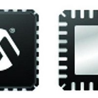
DSPIC33FJ32GP204-H/ML Microchip Technology, DSPIC33FJ32GP204-H/ML Datasheet - Page 270

DSPIC33FJ32GP204-H/ML
Manufacturer Part Number
DSPIC33FJ32GP204-H/ML
Description
16-bit DSC, 44LD,32KB Flash,40 MIPS,nanoWatt 44 QFN 8x8x0.9mm TUBE
Manufacturer
Microchip Technology
Series
dsPIC™ 33Fr
Datasheet
1.DSPIC33FJ16GP304-IPT.pdf
(284 pages)
Specifications of DSPIC33FJ32GP204-H/ML
Core Processor
dsPIC
Core Size
16-Bit
Speed
40 MIPs
Connectivity
I²C, IrDA, LIN, SPI, UART/USART
Peripherals
Brown-out Detect/Reset, POR, PWM, WDT
Number Of I /o
35
Program Memory Size
32KB (32K x 8)
Program Memory Type
FLASH
Ram Size
2K x 8
Voltage - Supply (vcc/vdd)
3 V ~ 3.6 V
Data Converters
A/D 13x12b
Oscillator Type
Internal
Operating Temperature
-40°C ~ 140°C
Package / Case
44-VQFN Exposed Pad
Processor Series
dsPIC33F
Core
dsPIC
Data Bus Width
16 bit
Interface Type
SPI, I2C, UART, JTAG
Number Of Programmable I/os
35
Operating Supply Voltage
3.3 V
Maximum Operating Temperature
+ 140 C
Mounting Style
SMD/SMT
Development Tools By Supplier
MPLAB IDE Software
Minimum Operating Temperature
- 40 C
On-chip Adc
10 bit, 13 Channel
Lead Free Status / RoHS Status
Lead free / RoHS Compliant
Eeprom Size
-
Lead Free Status / Rohs Status
Details
- Current page: 270 of 284
- Download datasheet (4Mb)
dsPIC33FJ32GP202/204 and dsPIC33FJ16GP304
TABLE A-1:
DS70290G-page 270
Section 14.0 “Serial Peripheral
Interface (SPI)”
Section 15.0 “Inter-Integrated
Circuit (I
Section 16.0 “Universal
Asynchronous Receiver Transmitter
(UART)”
Section 17.0 “10-bit/12-bit Analog-
to-Digital Converter (ADC)”
2
C™)”
Section Name
MAJOR SECTION UPDATES (CONTINUED)
Removed the following sections, which are now available in the related
section of the dsPIC33F/PIC24H Family Reference Manual:
• 14.1 “Interrupts”
• 14.2 “Receive Operations”
• 14.3 “Transmit Operations”
• 14.4 “SPI Setup” (retained Figure 14-1: SPI Module Block Diagram)
Removed the following sections, which are now available in the related
section of the dsPIC33F/PIC24H Family Reference Manual:
• 15.3 “I
• 15.4 “Baud Rate Generator” (retained Figure 15-1: I
• 15.5 “I
• 15.6 “Slave Address Masking”
• 15.7 “IPMI Support”
• 15.8 “General Call Address Support”
• 15.9 “Automatic Clock Stretch”
• 15.10 “Software Controlled Clock Stretching (STREN = 1)”
• 15.11 “Slope Control”
• 15.12 “Clock Arbitration”
• 15.13 “Multi-Master Communication, Bus Collision, and Bus Arbitration”
• 15.14 “Peripheral Pin Select Limitations”
Removed the following sections, which are now available in the related
section of the dsPIC33F/PIC24H Family Reference Manual:
• 16.1 “UART Baud Rate Generator”
• 16.2 “Transmitting in 8-bit Data Mode”
• 16.3 “Transmitting in 9-bit Data Mode”
• 16.4 “Break and Sync Transmit Sequence”
• 16.5 “Receiving in 8-bit or 9-bit Data Mode”
• 16.6 “Flow Control Using UxCTS and UxRTS Pins”
• 16.7 “Infrared Support”
Removed IrDA references and Note 1, and updated the bit and bit value
descriptions for UTXINV (UxSTA<14>) in the UARTx Status and Control
Register (see Register 16-2).
Removed Equation 17-1: ADC Conversion Clock Period and Figure 17-2:
ADC Transfer Function (10-Bit Example).
Added ADC1 Module Block Diagram for dsPIC33FJ16GP304 and
dsPIC33FJ32GP204 Devices (Figure 18-1) and ADC1 Module Block
Diagram FOR dsPIC33FJ32GP202 Devices (Figure 17-2).
Added Note 2 to Figure 17-3: ADC Conversion Clock Period Block Diagram.
Added device-specific information to Note 1 in the ADC1 Input Scan Select
Register Low (see Register 17-6), and updated the default bit value for bits
12-10 (CSS12-CSS10) from U-0 to R/W-0.
Added device-specific information to Note 1 in the ADC1 Port Configuration
Register Low (see Register 17-7), and updated the default bit value for bits
12-10 (PCFG12-PCFG10) from U-0 to R/W-0.
2
2
C Interrupts”
C Module Addresses”
Update Description
© 2011 Microchip Technology Inc.
2
C Block Diagram)
Related parts for DSPIC33FJ32GP204-H/ML
Image
Part Number
Description
Manufacturer
Datasheet
Request
R

Part Number:
Description:
IC, DSC, 16BIT, 12KB, 40MHZ, 3.6V, DIP28
Manufacturer:
Microchip Technology
Datasheet:

Part Number:
Description:
Manufacturer:
Microchip Technology Inc.
Datasheet:

Part Number:
Description:
Manufacturer:
Microchip Technology Inc.
Datasheet:

Part Number:
Description:
Manufacturer:
Microchip Technology Inc.
Datasheet:

Part Number:
Description:
Manufacturer:
Microchip Technology Inc.
Datasheet:

Part Number:
Description:
Manufacturer:
Microchip Technology Inc.
Datasheet:

Part Number:
Description:
Manufacturer:
Microchip Technology Inc.
Datasheet:

Part Number:
Description:
Manufacturer:
Microchip Technology Inc.
Datasheet:

Part Number:
Description:
Manufacturer:
Microchip Technology Inc.
Datasheet:


