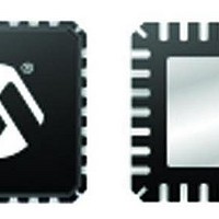
DSPIC33FJ32GP204-H/ML Microchip Technology, DSPIC33FJ32GP204-H/ML Datasheet - Page 247

DSPIC33FJ32GP204-H/ML
Manufacturer Part Number
DSPIC33FJ32GP204-H/ML
Description
16-bit DSC, 44LD,32KB Flash,40 MIPS,nanoWatt 44 QFN 8x8x0.9mm TUBE
Manufacturer
Microchip Technology
Series
dsPIC™ 33Fr
Datasheet
1.DSPIC33FJ16GP304-IPT.pdf
(284 pages)
Specifications of DSPIC33FJ32GP204-H/ML
Core Processor
dsPIC
Core Size
16-Bit
Speed
40 MIPs
Connectivity
I²C, IrDA, LIN, SPI, UART/USART
Peripherals
Brown-out Detect/Reset, POR, PWM, WDT
Number Of I /o
35
Program Memory Size
32KB (32K x 8)
Program Memory Type
FLASH
Ram Size
2K x 8
Voltage - Supply (vcc/vdd)
3 V ~ 3.6 V
Data Converters
A/D 13x12b
Oscillator Type
Internal
Operating Temperature
-40°C ~ 140°C
Package / Case
44-VQFN Exposed Pad
Processor Series
dsPIC33F
Core
dsPIC
Data Bus Width
16 bit
Interface Type
SPI, I2C, UART, JTAG
Number Of Programmable I/os
35
Operating Supply Voltage
3.3 V
Maximum Operating Temperature
+ 140 C
Mounting Style
SMD/SMT
Development Tools By Supplier
MPLAB IDE Software
Minimum Operating Temperature
- 40 C
On-chip Adc
10 bit, 13 Channel
Lead Free Status / RoHS Status
Lead free / RoHS Compliant
Eeprom Size
-
Lead Free Status / Rohs Status
Details
- Current page: 247 of 284
- Download datasheet (4Mb)
23.0
This section provides an overview of dsPIC33FJ32GP202/204 and dsPIC33FJ16GP304 electrical characteristics for
devices operating in an ambient temperature range of -40°C to +150°C.
The specifications between -40°C to +150°C are identical to those shown in
for operation between -40°C to +125°C, with the exception of the parameters listed in this section.
Parameters in this section begin with an H, which denotes High temperature. For example, parameter DC10 in
Section 22.0 “Electrical Characteristics”
Absolute maximum ratings for the dsPIC33FJ32GP202/204 and dsPIC33FJ16GP304 high temperature devices are
listed below. Exposure to these maximum rating conditions for extended periods can affect device reliability. Functional
operation of the device at these or any other conditions above the parameters indicated in the operation listings of this
specification is not implied.
Absolute Maximum Ratings
Ambient temperature under bias
Storage temperature .............................................................................................................................. -65°C to +160°C
Voltage on V
Voltage on any pin that is not 5V tolerant with respect to V
Voltage on any 5V tolerant pin with respect to V
Voltage on any 5V tolerant pin with respect to V
Voltage on V
Maximum current out of V
Maximum current into V
Maximum junction temperature............................................................................................................................. +155°C
Maximum output current sunk by any I/O pin
Maximum output current sourced by any I/O pin
Maximum current sunk by all ports combined ........................................................................................................10 mA
Maximum current sourced by all ports combined
© 2011 Microchip Technology Inc.
dsPIC33FJ32GP202/204 and dsPIC33FJ16GP304
Note:
Note 1: Stresses above those listed under “Absolute Maximum Ratings” can cause permanent damage to the
2: Maximum allowable current is a function of device maximum power dissipation (see
3: Unlike devices at 125°C and below, the specifications in this section also apply to the CLKOUT, V
4: AEC-Q100 reliability testing for devices intended to operate at 150°C is 1,000 hours. Any design in which
5: Refer to the
HIGH TEMPERATURE ELECTRICAL CHARACTERISTICS
Programming of the Flash memory is not allowed above 125°C.
device. This is a stress rating only, and functional operation of the device at those or any other conditions
above those indicated in the operation listings of this specification is not implied. Exposure to maximum
rating conditions for extended periods can affect device reliability.
V
the total operating time from 125°C to 150°C will be greater than 1,000 hours is not warranted without prior
written approval from Microchip Technology Inc.
DD
CAP
REF
with respect to V
with respect to V
-, SCLx, SDAx, PGCx, and PGDx pins.
DD
“Pin
SS
pin
pin .............................................................................................................................60 mA
(2)
Diagrams” section for 5V tolerant pins.
(4)
.............................................................................................................................60 mA
SS
SS
.........................................................................................................-40°C to +150°C
(1)
......................................................................................................... -0.3V to +4.0V
...................................................................................................... 2.25V to 2.75V
is the Industrial and Extended temperature equivalent of HDC10.
(3)
........................................................................................................1 mA
SS
SS
(3)
(2)
...................................................................................................1 mA
when V
when V
................................................................................................10 mA
SS
DD
DD
(5)
< 3.0V
≥ 3.0V
.................................................... -0.3V to (V
(5)
(5)
.................................................... -0.3V to 3.6V
.................................................... -0.3V to 5.6V
Section 22.0 “Electrical Characteristics”
Table
DS70290G-page 247
23-2).
DD
+ 0.3V)
REF
+,
Related parts for DSPIC33FJ32GP204-H/ML
Image
Part Number
Description
Manufacturer
Datasheet
Request
R

Part Number:
Description:
IC, DSC, 16BIT, 12KB, 40MHZ, 3.6V, DIP28
Manufacturer:
Microchip Technology
Datasheet:

Part Number:
Description:
Manufacturer:
Microchip Technology Inc.
Datasheet:

Part Number:
Description:
Manufacturer:
Microchip Technology Inc.
Datasheet:

Part Number:
Description:
Manufacturer:
Microchip Technology Inc.
Datasheet:

Part Number:
Description:
Manufacturer:
Microchip Technology Inc.
Datasheet:

Part Number:
Description:
Manufacturer:
Microchip Technology Inc.
Datasheet:

Part Number:
Description:
Manufacturer:
Microchip Technology Inc.
Datasheet:

Part Number:
Description:
Manufacturer:
Microchip Technology Inc.
Datasheet:

Part Number:
Description:
Manufacturer:
Microchip Technology Inc.
Datasheet:


