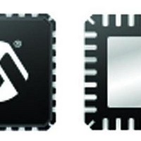
DSPIC33FJ32GP204-H/ML Microchip Technology, DSPIC33FJ32GP204-H/ML Datasheet - Page 227

DSPIC33FJ32GP204-H/ML
Manufacturer Part Number
DSPIC33FJ32GP204-H/ML
Description
16-bit DSC, 44LD,32KB Flash,40 MIPS,nanoWatt 44 QFN 8x8x0.9mm TUBE
Manufacturer
Microchip Technology
Series
dsPIC™ 33Fr
Datasheet
1.DSPIC33FJ16GP304-IPT.pdf
(284 pages)
Specifications of DSPIC33FJ32GP204-H/ML
Core Processor
dsPIC
Core Size
16-Bit
Speed
40 MIPs
Connectivity
I²C, IrDA, LIN, SPI, UART/USART
Peripherals
Brown-out Detect/Reset, POR, PWM, WDT
Number Of I /o
35
Program Memory Size
32KB (32K x 8)
Program Memory Type
FLASH
Ram Size
2K x 8
Voltage - Supply (vcc/vdd)
3 V ~ 3.6 V
Data Converters
A/D 13x12b
Oscillator Type
Internal
Operating Temperature
-40°C ~ 140°C
Package / Case
44-VQFN Exposed Pad
Processor Series
dsPIC33F
Core
dsPIC
Data Bus Width
16 bit
Interface Type
SPI, I2C, UART, JTAG
Number Of Programmable I/os
35
Operating Supply Voltage
3.3 V
Maximum Operating Temperature
+ 140 C
Mounting Style
SMD/SMT
Development Tools By Supplier
MPLAB IDE Software
Minimum Operating Temperature
- 40 C
On-chip Adc
10 bit, 13 Channel
Lead Free Status / RoHS Status
Lead free / RoHS Compliant
Eeprom Size
-
Lead Free Status / Rohs Status
Details
- Current page: 227 of 284
- Download datasheet (4Mb)
FIGURE 22-12:
TABLE 22-31: SPIx MASTER MODE (FULL-DUPLEX, CKE = 0, CKP = x, SMP = 1) TIMING
© 2011 Microchip Technology Inc.
AC CHARACTERISTICS
SP10
SP20
SP21
SP30
SP31
SP35
SP36
SP40
SP41
Note 1:
Param
dsPIC33FJ32GP202/204 and dsPIC33FJ16GP304
No.
(CKP = 0)
(CKP = 1)
SDIx
SCKx
SCKx
SDOx
Note: Refer to
2:
3:
4:
TscP
TscF
TscR
TdoF
TdoR
TscH2doV,
TscL2doV
TdoV2scH,
TdoV2scL
TdiV2scH,
TdiV2scL
TscH2diL,
TscL2diL
These parameters are characterized, but are not tested in manufacturing.
Data in “Typ” column is at 3.3V, 25°C unless otherwise stated.
The minimum clock period for SCKx is 111 ns. The clock generated in Master mode must not violate this
specification.
Assumes 50 pF load on all SPIx pins.
Symbol
Figure 22-1
REQUIREMENTS
SPIx MASTER MODE (FULL-DUPLEX, CKE = 0, CKP = X, SMP = 1) TIMING
CHARACTERISTICS
Maximum SCK Frequency
SCKx Output Fall Time
SCKx Output Rise Time
SDOx Data Output Fall Time
SDOx Data Output Rise Time
SDOx Data Output Valid after
SCKx Edge
SDOx Data Output Setup to
First SCKx Edge
Setup Time of SDIx Data
Input to SCKx Edge
Hold Time of SDIx Data Input
to SCKx Edge
SP30, SP31
for load conditions.
Characteristic
SP35
SP10
SP40 SP41
MSb In
MSb
(1)
Bit 14 - - - -1
Standard Operating Conditions: 3.0V to 3.6V
(unless otherwise stated)
Operating temperature
Bit 14 - - - - - -1
Min
—
—
30
30
30
—
—
—
—
Typ
SP21
SP20
—
—
—
—
—
—
—
—
6
SP30, SP31
(2)
Max
SP20
SP21
—
—
20
—
—
—
—
—
LSb In
9
LSb
-40°C ≤ T
-40°C ≤ T
Units
MHz
ns
ns
ns
ns
ns
ns
ns
ns
A
A
≤ +85°C for Industrial
≤ +125°C for Extended
-40ºC to +125ºC and
see Note 3
See parameter
and Note 4
See parameter
and Note 4
See parameter
and Note 4
See parameter
and Note 4
DS70290G-page 227
Conditions
—
—
—
—
DO32
DO31
DO32
DO31
Related parts for DSPIC33FJ32GP204-H/ML
Image
Part Number
Description
Manufacturer
Datasheet
Request
R

Part Number:
Description:
IC, DSC, 16BIT, 12KB, 40MHZ, 3.6V, DIP28
Manufacturer:
Microchip Technology
Datasheet:

Part Number:
Description:
Manufacturer:
Microchip Technology Inc.
Datasheet:

Part Number:
Description:
Manufacturer:
Microchip Technology Inc.
Datasheet:

Part Number:
Description:
Manufacturer:
Microchip Technology Inc.
Datasheet:

Part Number:
Description:
Manufacturer:
Microchip Technology Inc.
Datasheet:

Part Number:
Description:
Manufacturer:
Microchip Technology Inc.
Datasheet:

Part Number:
Description:
Manufacturer:
Microchip Technology Inc.
Datasheet:

Part Number:
Description:
Manufacturer:
Microchip Technology Inc.
Datasheet:

Part Number:
Description:
Manufacturer:
Microchip Technology Inc.
Datasheet:


