DSPIC33FJ32GP204-H/ML Microchip Technology, DSPIC33FJ32GP204-H/ML Datasheet - Page 279
DSPIC33FJ32GP204-H/ML
Manufacturer Part Number
DSPIC33FJ32GP204-H/ML
Description
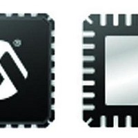
16-bit DSC, 44LD,32KB Flash,40 MIPS,nanoWatt 44 QFN 8x8x0.9mm TUBE
Manufacturer
Microchip Technology
Series
dsPIC™ 33Fr
Datasheet
1.DSPIC33FJ16GP304-IPT.pdf
(284 pages)
Specifications of DSPIC33FJ32GP204-H/ML
Core Processor
dsPIC
Core Size
16-Bit
Speed
40 MIPs
Connectivity
I²C, IrDA, LIN, SPI, UART/USART
Peripherals
Brown-out Detect/Reset, POR, PWM, WDT
Number Of I /o
35
Program Memory Size
32KB (32K x 8)
Program Memory Type
FLASH
Ram Size
2K x 8
Voltage - Supply (vcc/vdd)
3 V ~ 3.6 V
Data Converters
A/D 13x12b
Oscillator Type
Internal
Operating Temperature
-40°C ~ 140°C
Package / Case
44-VQFN Exposed Pad
Processor Series
dsPIC33F
Core
dsPIC
Data Bus Width
16 bit
Interface Type
SPI, I2C, UART, JTAG
Number Of Programmable I/os
35
Operating Supply Voltage
3.3 V
Maximum Operating Temperature
+ 140 C
Mounting Style
SMD/SMT
Development Tools By Supplier
MPLAB IDE Software
Minimum Operating Temperature
- 40 C
On-chip Adc
10 bit, 13 Channel
Lead Free Status / RoHS Status
Lead free / RoHS Compliant
Eeprom Size
-
Lead Free Status / Rohs Status
Details


Reset
Reset Sequence ................................................................. 71
Resets ................................................................................. 63
S
Serial Peripheral Interface (SPI) ....................................... 149
Software Reset Instruction (SWR) ...................................... 69
Software Simulator (MPLAB SIM)..................................... 201
Software Stack Pointer, Frame Pointer
Special Features of the CPU ............................................ 183
SPI Module
Symbols Used in Opcode Descriptions............................. 192
System Control
T
Temperature and Voltage Specifications
Timer1 ............................................................................... 135
Timer2/3, Timer4/5, Timer6/7 and Timer8/9 ..................... 137
Timing Characteristics
Timing Diagrams
© 2011 Microchip Technology Inc.
dsPIC33FJ32GP202/204 and dsPIC33FJ16GP304
PMD1 (Peripheral Module Disable Control
PMD2 (Peripheral Module Disable Control
RCON (Reset Control) ................................................ 64
SPIxCON1 (SPIx Control 1)...................................... 151
SPIxCON2 (SPIx Control 2)...................................... 153
SPIxSTAT (SPIx Status and Control) ....................... 150
SR (CPU Status)................................................... 22, 76
T1CON (Timer1 Control)........................................... 136
TxCON (T2CON, T4CON, T6CON or
TyCON (T3CON, T5CON, T7CON or
UxMODE (UARTx Mode).......................................... 164
UxSTA (UARTx Status and Control)......................... 166
Illegal Opcode ....................................................... 63, 70
Trap Conflict.......................................................... 69, 70
Uninitialized W Register........................................ 63, 70
CALL Stack Frame...................................................... 47
SPI1 Register Map...................................................... 40
Register Map............................................................... 46
AC ..................................................................... 213, 251
CLKO and I/O ........................................................... 217
10-bit A/D Conversion............................................... 244
10-bit A/D Conversion (CHPS = 01, SIMSAM = 0,
12-bit A/D Conversion (ASAM = 0, SSRC = 000) ..... 243
Brown-out Situations................................................... 69
External Clock........................................................... 214
Register 1) ........................................................ 111
Register 2) ........................................................ 112
T8CON Control) ................................................ 140
T9CON Control) ................................................ 141
ASAM = 0, SSRC = 000) .................................. 244
Timing Requirements
Timing Specifications
U
UART Module
Using the RCON Status Bits............................................... 70
V
Voltage Regulator (On-Chip) ............................................ 186
W
Watchdog Time-out Reset (WDTR).................................... 69
Watchdog Timer (WDT)............................................ 183, 187
WWW Address ................................................................. 281
WWW, On-Line Support ....................................................... 9
I2Cx Bus Data (Master Mode) .................................. 236
I2Cx Bus Data (Slave Mode) .................................... 238
I2Cx Bus Start/Stop Bits (Master Mode)................... 236
I2Cx Bus Start/Stop Bits (Slave Mode)..................... 238
Input Capture (CAPx) ............................................... 222
OC/PWM .................................................................. 223
Output Compare (OCx) ............................................ 222
Reset, Watchdog Timer, Oscillator Start-up Timer
Timer1, 2, 3, 4, 5, 6, 7, 8, 9 External Clock .............. 220
ADC Conversion (10-bit mode) ................................ 256
ADC Conversion (12-bit Mode) ................................ 256
CLKO and I/O ........................................................... 217
External Clock .......................................................... 214
Input Capture............................................................ 222
SPIx Master Mode (CKE = 0) ................................... 252
SPIx Module Master Mode (CKE = 1) ...................... 252
SPIx Module Slave Mode (CKE = 0) ........................ 253
SPIx Module Slave Mode (CKE = 1) ........................ 253
10-bit A/D Conversion Requirements ....................... 245
12-bit A/D Conversion Requirements ....................... 243
I2Cx Bus Data Requirements (Master Mode)........... 237
I2Cx Bus Data Requirements (Slave Mode)............. 239
Output Compare Requirements................................ 222
PLL Clock ......................................................... 215, 251
Reset, Watchdog Timer, Oscillator Start-up Timer,
Simple OC/PWM Mode Requirements ..................... 223
Timer1 External Clock Requirements....................... 220
Timer2 External Clock Requirements....................... 221
Timer3 External Clock Requirements....................... 221
UART1 Register Map ................................................. 40
Programming Considerations ................................... 187
and Power-up Timer ......................................... 218
Power-up Timer and Brown-out
Reset Requirements......................................... 219
DS70290G-page 279
Related parts for DSPIC33FJ32GP204-H/ML
Image
Part Number
Description
Manufacturer
Datasheet
Request
R

Part Number:
Description:
IC, DSC, 16BIT, 12KB, 40MHZ, 3.6V, DIP28
Manufacturer:
Microchip Technology
Datasheet:

Part Number:
Description:
Manufacturer:
Microchip Technology Inc.
Datasheet:
Part Number:
Description:
Manufacturer:
Microchip Technology Inc.
Datasheet:
Part Number:
Description:
Manufacturer:
Microchip Technology Inc.
Datasheet:
Part Number:
Description:
Manufacturer:
Microchip Technology Inc.
Datasheet:
Part Number:
Description:
Manufacturer:
Microchip Technology Inc.
Datasheet:
Part Number:
Description:
Manufacturer:
Microchip Technology Inc.
Datasheet:
Part Number:
Description:
Manufacturer:
Microchip Technology Inc.
Datasheet:
Part Number:
Description:
Manufacturer:
Microchip Technology Inc.
Datasheet: