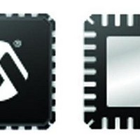
DSPIC33FJ32GP204-H/ML Microchip Technology, DSPIC33FJ32GP204-H/ML Datasheet - Page 251

DSPIC33FJ32GP204-H/ML
Manufacturer Part Number
DSPIC33FJ32GP204-H/ML
Description
16-bit DSC, 44LD,32KB Flash,40 MIPS,nanoWatt 44 QFN 8x8x0.9mm TUBE
Manufacturer
Microchip Technology
Series
dsPIC™ 33Fr
Datasheet
1.DSPIC33FJ16GP304-IPT.pdf
(284 pages)
Specifications of DSPIC33FJ32GP204-H/ML
Core Processor
dsPIC
Core Size
16-Bit
Speed
40 MIPs
Connectivity
I²C, IrDA, LIN, SPI, UART/USART
Peripherals
Brown-out Detect/Reset, POR, PWM, WDT
Number Of I /o
35
Program Memory Size
32KB (32K x 8)
Program Memory Type
FLASH
Ram Size
2K x 8
Voltage - Supply (vcc/vdd)
3 V ~ 3.6 V
Data Converters
A/D 13x12b
Oscillator Type
Internal
Operating Temperature
-40°C ~ 140°C
Package / Case
44-VQFN Exposed Pad
Processor Series
dsPIC33F
Core
dsPIC
Data Bus Width
16 bit
Interface Type
SPI, I2C, UART, JTAG
Number Of Programmable I/os
35
Operating Supply Voltage
3.3 V
Maximum Operating Temperature
+ 140 C
Mounting Style
SMD/SMT
Development Tools By Supplier
MPLAB IDE Software
Minimum Operating Temperature
- 40 C
On-chip Adc
10 bit, 13 Channel
Lead Free Status / RoHS Status
Lead free / RoHS Compliant
Eeprom Size
-
Lead Free Status / Rohs Status
Details
- Current page: 251 of 284
- Download datasheet (4Mb)
23.2
The information contained in this section defines
dsPIC33FJ32GP202/204 and dsPIC33FJ16GP304 AC
characteristics and timing parameters for high
temperature
specifications in this section are the same as those in
Section 22.2 “AC Characteristics and Timing
Parameters”, with the exception of the parameters
listed in this section.
TABLE 23-9:
FIGURE 23-1:
TABLE 23-10: PLL CLOCK TIMING SPECIFICATIONS
© 2011 Microchip Technology Inc.
AC CHARACTERISTICS
CHARACTERISTICS
HOS53
Note 1:
dsPIC33FJ32GP202/204 and dsPIC33FJ16GP304
Param
No.
AC Characteristics and Timing
Parameters
AC
These parameters are characterized by similarity, but are not tested in manufacturing. This specification is
based on clock cycle by clock cycle measurements. To calculate the effective jitter for individual time
bases or communication clocks use this formula::
D
For example: Fosc = 32 MHz, D
Symbol
CLK
devices.
Load Condition 1 – for all pins except OSC2
TEMPERATURE AND VOLTAGE SPECIFICATIONS – AC
LOAD CONDITIONS FOR DEVICE TIMING SPECIFICATIONS
CLKO Stability (Jitter)
Standard Operating Conditions: 3.0V to 3.6V (unless otherwise stated)
Operating temperature
However,
Pin
Characteristic
SPI SCK Jitter
all
Peripheral Clock Jitter
V
V
DD
AC
Standard Operating Conditions: 3.0V to 3.6V
(unless otherwise stated)
Operating temperature
Operating voltage V
SS
/2
CLK
(1)
R
C
L
timing
L
= 5%, SPI bit rate clock, (i.e., SCK) is 2 MHz.
-40°C ≤ T
=
Min
----------------------------- -
-5
⎛
⎝
32 MHz
------------------- -
D
2 MHz
A
CLK
≤ +150°C for High Temperature
=
R
C
DD
----------------------------------------------------------------------- -
Parameters in this section begin with an H, which
denotes High temperature. For example, parameter
OS53 in
Timing Parameters”
temperature equivalent of HOS53.
L
L
Typ
0.5
⎛
⎝
⎞
⎠
------------------------------------------------------------- -
Peripheral Bit Rate Clock
range as described in
= 464Ω
= 50 pF for all pins except OSC2
Load Condition 2 – for OSC2
-40°C ≤ T
=
15 pF for OSC2 output
Pin
--------- -
5%
Max
16
D
Section 22.2 “AC Characteristics and
F
5
CLK
OSC
A
=
≤ +150°C for High Temperature
5%
------- -
Units
4
%
is the Industrial and Extended
V
=
SS
Table
⎞
⎠
1.25%
Measured over 100 ms
period
C
L
23-1.
Conditions
DS70290G-page 251
Related parts for DSPIC33FJ32GP204-H/ML
Image
Part Number
Description
Manufacturer
Datasheet
Request
R

Part Number:
Description:
IC, DSC, 16BIT, 12KB, 40MHZ, 3.6V, DIP28
Manufacturer:
Microchip Technology
Datasheet:

Part Number:
Description:
Manufacturer:
Microchip Technology Inc.
Datasheet:

Part Number:
Description:
Manufacturer:
Microchip Technology Inc.
Datasheet:

Part Number:
Description:
Manufacturer:
Microchip Technology Inc.
Datasheet:

Part Number:
Description:
Manufacturer:
Microchip Technology Inc.
Datasheet:

Part Number:
Description:
Manufacturer:
Microchip Technology Inc.
Datasheet:

Part Number:
Description:
Manufacturer:
Microchip Technology Inc.
Datasheet:

Part Number:
Description:
Manufacturer:
Microchip Technology Inc.
Datasheet:

Part Number:
Description:
Manufacturer:
Microchip Technology Inc.
Datasheet:


