FDMA1029PZ Fairchild Semiconductor, FDMA1029PZ Datasheet
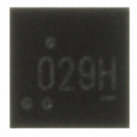
IC MOSFET P-CH DUAL MICROFET 2X2

FDMA1029PZ

Manufacturer Part Number
FDMA1029PZ
Description
IC MOSFET P-CH DUAL MICROFET 2X2
Manufacturer
Fairchild Semiconductor
Series
PowerTrench®r
Datasheet

Specifications of FDMA1029PZ

Fet Type
2 P-Channel (Dual)
Fet Feature
Logic Level Gate
Rds On (max) @ Id, Vgs
95 mOhm @ 3.1A, 4.5V
Drain To Source Voltage (vdss)
20V
Current - Continuous Drain (id) @ 25° C
3.1A
Vgs(th) (max) @ Id
1.5V @ 250µA
Gate Charge (qg) @ Vgs
10nC @ 4.5V
Input Capacitance (ciss) @ Vds
540pF @ 10V
Power - Max
700mW
Mounting Type
Surface Mount
Package / Case
6-MLP, 6-MicroFET™
Lead Free Status / RoHS Status
Lead free / RoHS Compliant
Other names
FDMA1029PZTR

Available stocks

Company
Part Number
Manufacturer
Quantity
Price
Part Number:
FDMA1029PZ
Manufacturer:
Fairchild Semiconductor
Quantity:
131 848
Part Number:
FDMA1029PZ
Manufacturer:
Fairchild
Quantity:
3 000
Part Number:
FDMA1029PZ
Manufacturer:
FAIRCHILD/仙童
Quantity:
20 000
FDMA1029PZ
Dual P-Channel PowerTrench
General Description
This device is designed specifically as a single package
solution for the battery charge switch in cellular handset
and other ultra-portable applications. It features two
independent P-Channel MOSFETs with low on-state
resistance for minimum conduction losses.
connected in the typical common source configuration,
bi-directional current flow is possible.
The MicroFET 2x2 package offers exceptional thermal
performance for its physical size and is well suited to
linear mode applications.
”2010 Fairchild Semiconductor Corporation
Absolute Maximum Ratings
Symbol
V
V
I
P
T
Thermal Characteristics
R
R
R
R
Package Marking and Ordering Information
D
J
DS
GS
D
TJA
TJA
TJA
TJA
, T
Device Marking
STG
029
Drain-Source Voltage
Gate-Source Voltage
Drain Current
Power Dissipation for Single Operation
Operating and Storage Junction Temperature Range
Thermal Resistance, Junction-to-Ambient
MicroFET 2x2
FDMA1029PZ
– Continuous
– Pulsed
D1 G2 S2
Device
Parameter
D1
PIN 1
S1 G1
D2
D2
T
When
MOSFET
A
=25
o
C unless otherwise noted
Reel Size
7’’
(Note 1a)
(Note 1a)
(Note 1b)
(Note 1a)
(Note 1b)
(Note 1c)
(Note 1d)
Features
x –3.1 A, –20V. R
x Low profile – 0.8 mm maximum – in the new package
x HBM ESD protection level > 2.5kV (Note 3)
x RoHS Compliant
Free from halogenated compounds and antimony
oxides
MicroFET 2x2 mm
S1
G1
D2
1
2
3
173 (Single Operation)
86 (Single Operation)
151 (Dual Operation)
69 (Dual Operation)
Tape width
R
DS(ON)
DS(ON)
–55 to +150
8mm
Ratings
–3.1
–20
r12
1.4
0.7
–6
= 95 m: @ V
= 141 m: @ V
FDMA1029PZ Rev.B4(W)
6
5
4
May 2010
GS
GS
D1
G2
S2
= –4.5V
3000 units
Quantity
= –2.5V
qC/W
Units
tm
qC
W
V
V
A
tm

Related parts for FDMA1029PZ

FDMA1029PZ Summary of contents

Page 1

... Operation) (Note 1b) 69 (Dual Operation) (Note 1c) 151 (Dual Operation) (Note 1d) Reel Size Tape width 7’’ May 2010 –4.5V DS(ON 141 –2.5V DS(ON Ratings Units –20 V r12 V A –3.1 –6 W 1.4 0.7 qC –55 to +150 qC/W Quantity 8mm 3000 units FDMA1029PZ Rev.B4(W) ...

Page 2

... 1.0 MHz V = – – –4 GEN V = – –3 –4 –1.1 A (Note –3 /dt = 100 A/µs F Min Typ Max Units –20 V mV/qC –12 PA –1 PA ±10 –0.6 –1.0 –1.5 V mV/ 141 87 140 –11 S 540 pF 120 pF 100 7 1.1 nC 2.4 nC -1.1 A –0.8 –1 FDMA1029PZ Rev.B4(W) ...

Page 3

... The diode connected between the gate and source serves only as protection against ESD. No gate overvoltage rating is implied. 2 oz. copper pad on a 1.5 x 1.5 in. board of FR-4 material b)173 C/W when mounted on a minimum pad copper. is guaranteed by design while R is determined by the TJC TJA o d)151 C/W when o c)69 C/W when mounted mounted minimum pad pad copper. copper. FDMA1029PZ Rev.B4(W) ...

Page 4

... Figure 6. Body Diode Forward Voltage Variation with Source Current and Temperature. = -2.0V -2.5V -3.0V -3.5V -4.0V -4. DRAIN CURRENT ( -1.55A 125 GATE TO SOURCE VOLTAGE (V) GS Gate-to-Source Voltage -55 C 0.4 0.6 0.8 1 1.2 1 BODY DIODE FORWARD VOLTAGE (V) SD FDMA1029PZ Rev.B4( 1.6 ...

Page 5

... Figure 10. Single Pulse Maximum Power 0.01 0 TIME (sec 1MHz iss C oss DRAIN TO SOURCE VOLTAGE (V) DS SINGLE PULSE R = 173°C/W TJA T = 25°C A 0.01 0 100 1000 Dissipation. R ( TJA TJA R =173 °C/W TJA P(pk (t) TJA J A Duty Cycle 100 1000 FDMA1029PZ Rev.B4(W) 20 ...

Page 6

... Dimensional Outline and Pad Layout ` FDMA1029PZ Rev.B4(W) ...

Page 7

... TinyBoost™ TinyBuck™ TinyCalc™ ® TinyLogic TINYOPTO™ TinyPower™ TinyPWM™ TinyWire™ TriFault Detect™ TRUECURRENT™* µSerDes™ ® UHC Ultra FRFET™ UniFET™ VCX™ VisualMax™ XS™ Definition FDMA1029PZ Rev.B4(W) ®* ® Rev. I48 ...

Related keywords