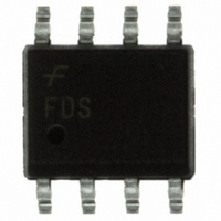
FDS4559 Fairchild Semiconductor, FDS4559 Datasheet - Page 3

FDS4559
Manufacturer Part Number
FDS4559
Description
MOSFET N/P-CH 60V 4.5/3.5A SO-8
Manufacturer
Fairchild Semiconductor
Series
PowerTrench®r
Datasheet
1.FDS4559.pdf
(8 pages)
Specifications of FDS4559
Fet Type
N and P-Channel
Fet Feature
Logic Level Gate
Rds On (max) @ Id, Vgs
55 mOhm @ 4.5A, 10V
Drain To Source Voltage (vdss)
60V
Current - Continuous Drain (id) @ 25° C
4.5A, 3.5A
Vgs(th) (max) @ Id
3V @ 250µA
Gate Charge (qg) @ Vgs
18nC @ 10V
Input Capacitance (ciss) @ Vds
650pF @ 25V
Power - Max
1W
Mounting Type
Surface Mount
Package / Case
8-SOIC (3.9mm Width)
Configuration
Dual Dual Drain
Transistor Polarity
N and P-Channel
Resistance Drain-source Rds (on)
0.055 Ohm @ 10 V @ N Channel
Forward Transconductance Gfs (max / Min)
14 S, 9 S
Drain-source Breakdown Voltage
60 V
Gate-source Breakdown Voltage
+/- 20 V
Continuous Drain Current
4.5 A @ N Channel or 3.5 A @ P Channel
Power Dissipation
2000 mW
Maximum Operating Temperature
+ 175 C
Mounting Style
SMD/SMT
Minimum Operating Temperature
- 55 C
Lead Free Status / RoHS Status
Lead free / RoHS Compliant
Other names
FDS4559
FDS4559TR
FDS4559TR
Available stocks
Company
Part Number
Manufacturer
Quantity
Price
Company:
Part Number:
FDS4559
Manufacturer:
FSC
Quantity:
50 000
Company:
Part Number:
FDS4559
Manufacturer:
FSC
Quantity:
45 000
Part Number:
FDS4559
Manufacturer:
FAIRCHILD/仙童
Quantity:
20 000
Company:
Part Number:
FDS4559-NL
Manufacturer:
FSC
Quantity:
45 500
Company:
Part Number:
FDS4559-NL
Manufacturer:
FSC
Quantity:
50 000
Part Number:
FDS4559-NL
Manufacturer:
FAIRCHILD/仙童
Quantity:
20 000
Part Number:
FDS4559_NL
Manufacturer:
FAIRCHILD/仙童
Quantity:
20 000
Notes:
1. R
Scale 1 : 1 on letter size paper
2. Pulse Test: Pulse Width < 300 s, Duty Cycle < 2.0%
Electrical Characteristics
Symbol
Drain-Source Diode Characteristics and Maximum Ratings
I
V
S
the drain pins. R
SD
JA
is the sum of the junction-to-case and case-to-ambient thermal resistance where the case thermal reference is defined as the solder mounting surface of
Voltage
Maximum Continuous Drain-Source Diode Forward Current
Drain-Source Diode Forward
JC
is guaranteed by design while R
Parameter
a) 78°C/W when
mounted on a
0.5 in
copper
2
pad of 2 oz
CA
V
V
(continued)
GS
GS
is determined by the user's board design.
= 0 V, I
= 0 V, I
Test Conditions
b) 125°C/W when
S
S
= 1.3 A
= –1.3 A
mounted on a .02 in
pad of 2 oz copper
T
A
= 25°C unless otherwise noted
(Note 2)
(Note 2)
2
Type Min
Q1
Q2
Q1
Q2
c) 135°C/W when mounted on a
minimum pad.
Typ Max Units
–0.8
0.8
–1.3
–1.2
1.3
1.2
FDS4559 Rev C1(W)
A
V


