FDC6301N Fairchild Semiconductor, FDC6301N Datasheet
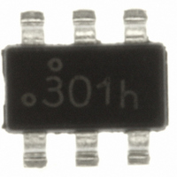
IC FET DGTL N-CH DUAL 25V SSOT6

FDC6301N

Manufacturer Part Number
FDC6301N
Description
IC FET DGTL N-CH DUAL 25V SSOT6
Manufacturer
Fairchild Semiconductor
Datasheet

Specifications of FDC6301N

Fet Type
2 N-Channel (Dual)
Fet Feature
Logic Level Gate
Rds On (max) @ Id, Vgs
4 Ohm @ 400mA, 4.5V
Drain To Source Voltage (vdss)
25V
Current - Continuous Drain (id) @ 25° C
220mA
Vgs(th) (max) @ Id
1.5V @ 250µA
Gate Charge (qg) @ Vgs
0.7nC @ 4.5V
Input Capacitance (ciss) @ Vds
9.5pF @ 10V
Power - Max
700mW
Mounting Type
Surface Mount
Package / Case
6-SSOT, SuperSOT-6
Configuration
Dual
Transistor Polarity
N-Channel
Resistance Drain-source Rds (on)
4 Ohm @ 4.5 V
Forward Transconductance Gfs (max / Min)
0.25 S
Drain-source Breakdown Voltage
25 V
Gate-source Breakdown Voltage
- 0.5 V to 8 V
Continuous Drain Current
0.22 A
Power Dissipation
900 mW
Maximum Operating Temperature
+ 150 C
Mounting Style
SMD/SMT
Minimum Operating Temperature
- 55 C
Continuous Drain Current Id
220mA
Drain Source Voltage Vds
25V
On Resistance Rds(on)
5ohm
Rds(on) Test Voltage Vgs
4.5V
Threshold Voltage Vgs Typ
850mV
Rohs Compliant
Yes
Lead Free Status / RoHS Status
Lead free / RoHS Compliant
Other names
FDC6301NTR

Available stocks

Company
Part Number
Manufacturer
Quantity
Price
Part Number:
FDC6301N
Manufacturer:
Fairchild Semiconductor
Quantity:
37 261
Part Number:
FDC6301N
Manufacturer:
FSC
Quantity:
8 000
Part Number:
FDC6301N
Manufacturer:
FAIRCHILD/仙童
Quantity:
20 000
Part Number:
FDC6301N
0
Company:
Part Number:
FDC6301N
Quantity:
30 000
Company:
Part Number:
FDC6301N
Quantity:
15 000
Company:
Part Number:
FDC6301N
Quantity:
18 000
Company:
Part Number:
FDC6301N
Quantity:
5 000
Part Number:
FDC6301N-NL
Manufacturer:
FAIRCHILD/仙童
Quantity:
20 000
Symbol
V
V
I
P
T
ESD
THERMAL CHARACTERISTICS
R
R
© 2001 Fairchild Semiconductor Corporation
D
Absolute Maximum Ratings
DSS
GSS
, I
D
J
General Description
These dual N-Channel logic level enhancement mode field
effect transistors are produced using Fairchild 's proprietary,
high cell density, DMOS technology. This very high density
process is especially tailored to minimize on-state resistance.
This
applications as a replacement for digital transistors. Since bias
resistors are not required, these N-Channel FET's can replace
several digital transistors, with a variety of bias resistors.
,T
FDC6301N
Dual N-Channel , Digital FET
JA
JC
OUT
STG
, V
, V
SOT-23
CC
IN
device has been designed especially for low voltage
Parameter
Drain-Source Voltage, Power Supply Voltage
Gate-Source Voltage, V
Drain/Output Current
Maximum Power Dissipation
Operating and Storage Temperature Range
Electrostatic Discharge Rating MIL-STD-883D
Human Body Model (100pf / 1500 Ohm)
Thermal Resistance, Junction-to-Ambient
Thermal Resistance, Junction-to-Case
SuperSOT
Mark: .301
IN
TM
-6
- Continuous
- Pulsed
T
A
= 25
o
C unless other wise noted
SuperSOT
(Note 1a)
(Note 1a)
(Note 1b)
(Note 1)
6
4
5
TM
-8
Features
SO-8
25 V, 0.22 A continuous, 0.5 A Peak.
Very low level gate drive requirements allowing direct
operation in 3V circuits. V
Gate-Source Zener for ESD ruggedness.
>6kV Human Body Model.
2
1
3
R
R
DS(ON)
DS(ON)
- 0.5 to +8
FDC6301N
-55 to 150
IN
= 4
0.22
= 5
140
6.0
0.5
0.9
0.7
25
60
SOT-223
@ V
@ V
GS(th)
I N V E R T E R A P P L I C A T I O N
GS
GS
< 1.5V.
= 4.5 V.
= 2.7 V
G
D
September 2001
SOIC-16
S
FDC6301N Rev.D
Units
°C/W
°C/W
°C
kV
W
V
V
A
Vcc
O U T
GND

Related parts for FDC6301N

FDC6301N Summary of contents

Page 1

... Human Body Model. TM SuperSOT -8 SO unless other wise noted A (Note 1a) (Note 1b) (Note 1a) (Note 1) September 2001 2.7 V DS(ON 4.5 V. DS(ON) GS < 1.5V. GS(th) SOIC-16 SOT-223 FDC6301N 0.22 0.5 0.9 0.7 -55 to 150 6.0 140 60 FDC6301N Rev.D Vcc GND Units °C kV °C/W °C/W ...

Page 2

... FR-4 in still air 180 C 0.005 in of pad of 2oz copper. Min Typ Max Units 55°C J 100 o -2 0.65 0.85 1.5 3 =125°C 6 3.1 4 0.2 0.25 9 3.2 7 0.49 0.7 0.22 0.07 1 0 guaranteed by JC FDC6301N Rev µA µ µ ...

Page 3

... I , DRAIN CURRENT (A) D Drain Current and Gate Voltage 0.2A D 125°C 3 3 GATE TO SOURCE VOLTAGE ( Resistance Variation with = 125°C J 25°C -55°C 0.4 0.6 0 BODY DIODE FORWARD VOLTAGE (V) SD Body Diode Forward Voltage FDC6301N Rev.D 0.5 5 1.2 ...

Page 4

... Figure 10. Single Pulse Maximum Power 0.01 0 TIME (sec iss C oss = 0V C rss 0 DRAIN TO SOURCE VOLTAGE (V) DS SINGLE PULSE R =See note 25° SINGLE PULSE TIME (SEC) Dissipation. R ( See Note 1b JA P(pk ( Duty Cycle 100 FDC6301N Rev 100 300 300 ...

Page 5

CROSSVOLT â â â â Rev. H5 ...

Related keywords