FDG6317NZ Fairchild Semiconductor, FDG6317NZ Datasheet
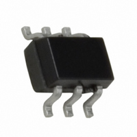
MOSFET N-CH DUAL 20V SC70-6

FDG6317NZ

Manufacturer Part Number
FDG6317NZ
Description
MOSFET N-CH DUAL 20V SC70-6
Manufacturer
Fairchild Semiconductor
Series
PowerTrench®r
Type
Power MOSFETr
Datasheet

Specifications of FDG6317NZ

Fet Type
2 N-Channel (Dual)
Fet Feature
Logic Level Gate
Rds On (max) @ Id, Vgs
400 mOhm @ 700mA, 4.5V
Drain To Source Voltage (vdss)
20V
Current - Continuous Drain (id) @ 25° C
700mA
Vgs(th) (max) @ Id
1.5V @ 250µA
Gate Charge (qg) @ Vgs
1.1nC @ 4.5V
Input Capacitance (ciss) @ Vds
66.5pF @ 10V
Power - Max
300mW
Mounting Type
Surface Mount
Package / Case
SC-70-6, SC-88, SOT-363
Configuration
Dual
Transistor Polarity
N-Channel
Resistance Drain-source Rds (on)
0.4 Ohm @ 4.5 V
Forward Transconductance Gfs (max / Min)
1.8 S
Drain-source Breakdown Voltage
20 V
Gate-source Breakdown Voltage
+/- 12 V
Continuous Drain Current
0.7 A
Power Dissipation
300 mW
Maximum Operating Temperature
+ 150 C
Mounting Style
SMD/SMT
Minimum Operating Temperature
- 55 C
Number Of Elements
2
Polarity
N
Channel Mode
Enhancement
Drain-source On-res
0.4Ohm
Drain-source On-volt
20V
Gate-source Voltage (max)
±12V
Output Power (max)
Not RequiredW
Frequency (max)
Not RequiredMHz
Noise Figure
Not RequireddB
Power Gain
Not RequireddB
Drain Efficiency
Not Required%
Operating Temp Range
-55C to 150C
Operating Temperature Classification
Military
Mounting
Surface Mount
Pin Count
6
Package Type
SC-70
Lead Free Status / RoHS Status
Lead free / RoHS Compliant

Available stocks

Company
Part Number
Manufacturer
Quantity
Price
Part Number:
FDG6317NZ
Manufacturer:
FSC
Quantity:
36 000
Part Number:
FDG6317NZ
Manufacturer:
FAIRCHILD/仙童
Quantity:
20 000
Part Number:
FDG6317NZ
0
Company:
Part Number:
FDG6317NZ
Quantity:
30 000
Company:
Part Number:
FDG6317NZ
Quantity:
400
©2009 Fairchild Semiconductor Corporation
FDG6317NZ Rev.B1 (W)
FDG6317NZ
Dual 20v N-Channel PowerTrench MOSFET
General Description
This dual N-Channel MOSFET has been designed
specifically to improve the overall efficiency of DC/DC
converters using either synchronous or conventional
switching PWM controllers. It has been optimized use
in small switching regulators, providing an extremely
low R
Applications
Absolute Maximum Ratings
Symbol
V
V
I
P
T
Thermal Characteristics
R
Package Marking and Ordering Information
RoHS Compliant
D
DC/DC converter
Power management
Load switch
J
DSS
GSS
D
, T
JA
Device Marking
DS(ON)
STG
and gate charge (Q
.67
Drain-Source Voltage
Gate-Source Voltage
Drain Current
Power Dissipation for Single Operation
Operating and Storage Junction Temperature Range
Thermal Resistance, Junction-to-Ambient
D
Pin 1
G
S
SC70-6
G
) in a small package.
– Continuous
– Pulsed
The pinouts are symmetrical; pin 1 and pin 4 are interchangeable.
FDG6317NZ
S
Device
Parameter
G
D
T
A
=25
o
C unless otherwise noted
Reel Size
1
7’’
(Note 1)
(Note 1)
(Note 1)
Features
0.7 A, 20 V.
Gate-Source Zener for ESD ruggedness
(1.6kV Human Body Model). (Note 3)
Low gate charge
High performance trench technology for extremely
low R
Compact industry standard SC70-6 surface mount
package
DS(ON)
Tape width
–55 to +150
8mm
R
R
Ratings
DS(ON)
DS(ON)
415
0.7
2.1
0.3
20
12
= 400 m @ V
= 550 m @ V
May 2009
www.fairchildsemi.com
GS
GS
3000 units
Quantity
= 4.5 V
= 2.5 V
Units
C/W
W
V
V
A
C

Related parts for FDG6317NZ

FDG6317NZ Summary of contents

Page 1

... Thermal Resistance, Junction-to-Ambient JA Package Marking and Ordering Information Device Marking Device .67 FDG6317NZ ©2009 Fairchild Semiconductor Corporation FDG6317NZ Rev.B1 (W) Features 0 Gate-Source Zener for ESD ruggedness (1.6kV Human Body Model). (Note 3) Low gate charge High performance trench technology for extremely low R Compact industry standard SC70-6 surface mount ...

Page 2

... R is guaranteed by design while Pulse Test: Pulse Width < 300 s, Duty Cycle < 2.0% 3. The diode connected between the gate and source serves only as protection against ESD. No gate overvoltage rating is implied. ©2009 Fairchild Semiconductor Corporation FDG6317NZ Rev.B1 ( 25°C unless otherwise noted A Test Conditions V ...

Page 3

... Figure 3. On-Resistance Variation with Temperature 125 1 GATE TO SOURCE VOLTAGE (V) GS Figure 5. Transfer Characteristics. ©2009 Fairchild Semiconductor Corporation FDG6317NZ Rev.B1 (W) 1.7 2.5V 1.5 1.3 2.0V 1.1 0.9 0 1.5 2 2.5 Figure 2. On-Resistance Variation with 1 0.8 0.6 0.4 0.2 75 100 125 150 ...

Page 4

... DRAIN-SOURCE VOLTAGE (V) DS Figure 9. Maximum Safe Operating Area 0.5 0.2 0.1 0.1 0.05 0.02 0.01 SINGLE PULSE 0.01 0.0001 0.001 Figure 11. Transient Thermal Response Curve. ©2009 Fairchild Semiconductor Corporation FDG6317NZ Rev.B1 (W) 100 15V 75 10V 0.6 0 Figure 8. Capacitance Characteristics. 10 100 s 8 1ms ...

Page 5

... Datasheet Identification Product Status Advance Information Formative / In Design Preliminary First Production No Identification Needed Full Production Obsolete Not In Production ©2009 Fairchild Semiconductor Corporation FDG6317NZ Rev.B1 (W) F-PFS™ PowerTrench ® FRFET PowerXS™ SM Global Power Resource Programmable Active Droop™ ® Green FPS™ ...

Related keywords