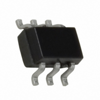
FDG6317NZ Fairchild Semiconductor, FDG6317NZ Datasheet - Page 4

FDG6317NZ
Manufacturer Part Number
FDG6317NZ
Description
MOSFET N-CH DUAL 20V SC70-6
Manufacturer
Fairchild Semiconductor
Series
PowerTrench®r
Type
Power MOSFETr
Datasheet
1.FDG6317NZ.pdf
(5 pages)
Specifications of FDG6317NZ
Fet Type
2 N-Channel (Dual)
Fet Feature
Logic Level Gate
Rds On (max) @ Id, Vgs
400 mOhm @ 700mA, 4.5V
Drain To Source Voltage (vdss)
20V
Current - Continuous Drain (id) @ 25° C
700mA
Vgs(th) (max) @ Id
1.5V @ 250µA
Gate Charge (qg) @ Vgs
1.1nC @ 4.5V
Input Capacitance (ciss) @ Vds
66.5pF @ 10V
Power - Max
300mW
Mounting Type
Surface Mount
Package / Case
SC-70-6, SC-88, SOT-363
Configuration
Dual
Transistor Polarity
N-Channel
Resistance Drain-source Rds (on)
0.4 Ohm @ 4.5 V
Forward Transconductance Gfs (max / Min)
1.8 S
Drain-source Breakdown Voltage
20 V
Gate-source Breakdown Voltage
+/- 12 V
Continuous Drain Current
0.7 A
Power Dissipation
300 mW
Maximum Operating Temperature
+ 150 C
Mounting Style
SMD/SMT
Minimum Operating Temperature
- 55 C
Number Of Elements
2
Polarity
N
Channel Mode
Enhancement
Drain-source On-res
0.4Ohm
Drain-source On-volt
20V
Gate-source Voltage (max)
±12V
Output Power (max)
Not RequiredW
Frequency (max)
Not RequiredMHz
Noise Figure
Not RequireddB
Power Gain
Not RequireddB
Drain Efficiency
Not Required%
Operating Temp Range
-55C to 150C
Operating Temperature Classification
Military
Mounting
Surface Mount
Pin Count
6
Package Type
SC-70
Lead Free Status / RoHS Status
Lead free / RoHS Compliant
Available stocks
Company
Part Number
Manufacturer
Quantity
Price
Company:
Part Number:
FDG6317NZ
Manufacturer:
FSC
Quantity:
36 000
Part Number:
FDG6317NZ
Manufacturer:
FAIRCHILD/仙童
Quantity:
20 000
©2009 Fairchild Semiconductor Corporation
FDG6317NZ Rev.B1 (W)
Typical Characteristics
0.001
5
4
3
2
1
0
0.01
0.1
10
0
1
Figure 9. Maximum Safe Operating Area.
0.1
Figure 7. Gate Charge Characteristics.
I
0.01
D
0.1
= 0.7A
R
0.0001
SINGLE PULSE
1
DS(ON)
R
JA
V
T
0.2
GS
A
= 415
D = 0.5
LIMIT
= 25
= 10V
o
o
V
C
0.2
C/W
DS
0.1
, DRAIN-SOURCE VOLTAGE (V)
0.05
Q
0.02
g
1
, GATE CHARGE (nC)
0.4
0.01
0.001
V
SINGLE PULSE
DS
DC
= 5V
1s
100m
Figure 11. Transient Thermal Response Curve.
0.6
Thermal characterization performed using the conditions described in Note 1.
Transient thermal response will change depending on the circuit board design.
10ms
10
10V
1ms
0.01
100 s
0.8
15V
100
1
0.1
t
4
1
, TIME (sec)
100
10
0.0001
75
50
25
8
6
4
2
0
0
0
Figure 8. Capacitance Characteristics.
1
Figure 10. Single Pulse Maximum
C
0.001
rss
V
DS
Power Dissipation.
5
0.01
, DRAIN TO SOURCE VOLTAGE (V)
C
10
oss
t
0.1
1
, TIME (sec)
10
P(pk
Duty Cycle, D = t
T
R
1
J
R
- T
)
JA
JA
(t) = r(t)*R
C
A
= 415°C/W
= P * R
100
iss
t
1
10
t
2
SINGLE PULSE
R
15
JA
T
www.fairchildsemi.com
JA
A
1
= 415°C/W
JA
(t)
= 25°C
/ t
100
2
V
f = 1MHz
GS
= 0 V
1000
1000
20


