FDS6993 Fairchild Semiconductor, FDS6993 Datasheet
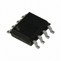
MOSFET P-CH DUAL 30/12V 8SOIC

FDS6993

Manufacturer Part Number
FDS6993
Description
MOSFET P-CH DUAL 30/12V 8SOIC
Manufacturer
Fairchild Semiconductor
Series
PowerTrench®r
Datasheet

Specifications of FDS6993

Fet Type
2 P-Channel (Dual)
Fet Feature
Logic Level Gate
Rds On (max) @ Id, Vgs
55 mOhm @ 4.3A, 10V
Drain To Source Voltage (vdss)
30V, 12V
Current - Continuous Drain (id) @ 25° C
4.3A, 6.8A
Vgs(th) (max) @ Id
3V @ 250µA
Gate Charge (qg) @ Vgs
7.7nC @ 5V
Input Capacitance (ciss) @ Vds
530pF @ 15V
Power - Max
900mW
Mounting Type
Surface Mount
Package / Case
8-SOIC (3.9mm Width)
Configuration
Dual Dual Drain
Transistor Polarity
P-Channel
Resistance Drain-source Rds (on)
0.055 Ohms
Drain-source Breakdown Voltage
- 30 V, + 12 V
Gate-source Breakdown Voltage
+/- 25 V, +/- 8 V
Continuous Drain Current
4.3 A, - 6.8 A
Power Dissipation
2 W
Maximum Operating Temperature
+ 150 C
Mounting Style
SMD/SMT
Minimum Operating Temperature
- 55 C
Lead Free Status / RoHS Status
Lead free / RoHS Compliant

Available stocks

Company
Part Number
Manufacturer
Quantity
Price
Part Number:
FDS6993
Manufacturer:
FSC
Quantity:
63 600
Part Number:
FDS6993
Manufacturer:
FSC
Quantity:
371
Part Number:
FDS6993-NL
Manufacturer:
FSC
Quantity:
60 000
Part Number:
FDS6993-NL
Manufacturer:
MCC
Quantity:
15 000
Part Number:
FDS6993-NL
Manufacturer:
FAIRCHILD
Quantity:
50 000
FDS6993
Dual P-Channel PowerTrench MOSFET
General Description
These P-Channel MOSFETs are made
using FSC’s PowerTrench technology.
They are packaged in a single SO-8 which is
designed to allow two MOSFETs to operate
independenly, each with it’s own heat sink.
The combination of silicon and package
technologies results in minimum board
space and cost.
2003 Fairchild Semiconductor Corporation
Absolute Maximum Ratings
V
V
I
P
T
Thermal Characteristics
R
R
Package Marking and Ordering Information
Symbol
D
J
DSS
GSS
D
, T
JA
JC
Device Marking
STG
FDS6993
SO-8
Drain-Source Voltage
Gate-Source Voltage
Drain Current
Power Dissipation for Dual Operation
Power Dissipation for Single Operation
Operating and Storage Junction Temperature Range
Thermal Resistance, Junction-to-Ambient
Thermal Resistance, Junction-to-Case
D
D1
Pin 1
D
D1
SO-8
D
D2
- Continuous
- Pulsed
D
FDS6993
D2
Device
Parameter
S1
S
G1
S
S2
S
G2
T
G
A
= 25°C unless otherwise noted
Reel Size
13”
(Note 1a)
(Note 1a)
(Note 1b)
(Note 1c)
(Note 1a)
(Note 1)
Features
Q1:
–4.3A, –30V R
Q2:
–6.8A, –12V R
High power and handling capability in a widely
used surface mount package
5
6
7
8
P-Channel
P-Channel
–4.3
Q1
–30
–20
Q2
Q1
25
Tape width
R
R
R
–55 to +150
12mm
DS(on)
DS(on)
DS(on)
DS(on)
DS(on)
1.6
0.9
78
40
2
1
= 55m
= 85m
= 17m
= 24m
= 30m
4
3
2
1
–6.8
Q2
–12
–20
@ V
@ V
@ V
@ V
@ V
8
June 2003
GS
GS
GS
GS
GS
= –10V
= –4.5V
= –4.5V
= –2.5V
= –1.8V
2500 units
FDS6993 Rev C (W)
Quantity
Units
C/W
C/W
W
V
V
A
C

Related parts for FDS6993

FDS6993 Summary of contents

Page 1

... June 2003 P-Channel = 55m @ V = –10V DS(on 85m @ V = –4.5V DS(on) GS P-Channel = 17m @ V = –4.5V DS(on 24m @ V = –2.5V DS(on 30m @ V = –1.8V DS(on Units –30 – –4.3 –6.8 A –20 – 1.6 1 0.9 –55 to +150 C 78 C/W 40 C/W Tape width Quantity 12mm 2500 units FDS6993 Rev C (W) ...

Page 2

... – – 1.0 MHz – 1.0 MHz DS GS Type Min Typ Max Units Q1 – –12 Q1 –21 mV –0.9 Q1 – –1 Q1 ±100 nA Q2 ±100 Q1 –1 –1.8 – –0.4 –0.5 –1 mV – – 530 pF Q2 2980 Q1 140 pF Q2 1230 790 FDS6993 Rev C (W) ...

Page 3

... CA b) 125°/W when 2 mounted on a .02 in pad copper Type Min Typ Max Units 134 215 121 193 Q1 5 4 8.0 Q1 –1 –1.3 Q1 –0.8 –1 –0.6 –1.2 c) 135°/W when mounted on a minimum pad. FDS6993 Rev C (W) ...

Page 4

... Figure 6. Body Diode Forward Voltage Variation with Source Current and Temperature. =-4.0V -4.5V -5.0V -6.0V -7.0V -8.0V -10V DRAIN CURRENT ( -2.15A 125 7 GATE TO SOURCE VOLTAGE (V) GS Gate-to-Source Voltage. = 125 -55 C 0.2 0.4 0.6 0 BODY DIODE FORWARD VOLTAGE (V) SD FDS6993 Rev C ( 1.4 ...

Page 5

... Figure 10. Single Pulse Maximum 0.01 0 TIME (sec MHz iss C oss DRAIN TO SOURCE VOLTAGE (V) DS SINGLE PULSE R = 135°C 25° 100 1000 t , TIME (sec) 1 Power Dissipation. R ( 135 C/W JA P(pk ( Duty Cycle 100 1000 FDS6993 Rev C (W) 30 ...

Page 6

... C 0.0001 0 1.6 2 Figure 17. Body Diode Forward Voltage Variation with Source Current and Temperature. -3.0V -3.5V -4.5V -6.0V -10. DRAIN CURRENT ( -3. 125 GATE TO SOURCE VOLTAGE (V) GS Gate-to-Source Voltage 125 -55 C 0.2 0.4 0.6 0 BODY DIODE FORWARD VOLTAGE (V) SD FDS6993 Rev C ( ...

Page 7

... Figure 21. Single Pulse Maximum 0.01 0 TIME (sec MHz iss C oss rss DRAIN TO SOURCE VOLTAGE (V) DS SINGLE PULSE R = 135°C 25° 100 t , TIME (sec) 1 Power Dissipation. R ( 135 C/W JA P(pk ( Duty Cycle 100 1000 FDS6993 Rev C (W) 12 1000 ...

Page 8

... FDS6993 Rev C (W) ...

Related keywords