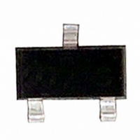
NDS356AP Fairchild Semiconductor, NDS356AP Datasheet - Page 3

NDS356AP
Manufacturer Part Number
NDS356AP
Description
MOSFET P-CH 30V 1.1A SSOT3
Manufacturer
Fairchild Semiconductor
Type
Power MOSFETr
Datasheet
1.NDS356AP.pdf
(7 pages)
Specifications of NDS356AP
Fet Type
MOSFET P-Channel, Metal Oxide
Fet Feature
Logic Level Gate
Rds On (max) @ Id, Vgs
200 mOhm @ 1.3A, 10V
Drain To Source Voltage (vdss)
30V
Current - Continuous Drain (id) @ 25° C
1.1A
Vgs(th) (max) @ Id
2.5V @ 250µA
Gate Charge (qg) @ Vgs
4.4nC @ 5V
Input Capacitance (ciss) @ Vds
280pF @ 10V
Power - Max
460mW
Mounting Type
Surface Mount
Package / Case
3-SSOT, SuperSOT-3
Number Of Elements
1
Polarity
P
Channel Mode
Enhancement
Drain-source On-res
0.2Ohm
Drain-source On-volt
30V
Gate-source Voltage (max)
±20V
Drain Current (max)
1.1A
Power Dissipation
500mW
Output Power (max)
Not RequiredW
Frequency (max)
Not RequiredMHz
Noise Figure
Not RequireddB
Power Gain
Not RequireddB
Drain Efficiency
Not Required%
Operating Temp Range
-55C to 150C
Operating Temperature Classification
Military
Mounting
Surface Mount
Pin Count
3
Package Type
SuperSOT
Lead Free Status / RoHS Status
Lead free / RoHS Compliant
Other names
NDS356APTR
Available stocks
Company
Part Number
Manufacturer
Quantity
Price
Company:
Part Number:
NDS356AP
Manufacturer:
FSC
Quantity:
255 000
Company:
Part Number:
NDS356AP
Manufacturer:
FAIRCHILD
Quantity:
5 321
Part Number:
NDS356AP
Manufacturer:
FAIRCHILD/仙童
Quantity:
20 000
Part Number:
NDS356AP-NL
Manufacturer:
FAIRCHILD/仙童
Quantity:
20 000
Part Number:
NDS356AP_NL
Manufacturer:
FAIRCHILD/仙童
Quantity:
20 000
Electrical Characteristics
Symbol
DRAIN-SOURCE DIODE CHARACTERISTICS AND MAXIMUM RATINGS
I
I
V
2. Pulse Test: Pulse Width < 300µs, Duty Cycle < 2.0%.
S
SM
1. R
Notes:
SD
Typical R
design while R
P
JA
D
is the sum of the junction-to-case and case-to-ambient thermal resistance where the case thermal reference is defined as the solder mounting surface of the drain pins. R
t
JA
a. 250
b. 270
Scale 1 : 1 on letter size paper
using the board layouts shown below on 4.5"x5" FR-4 PCB in a still air environment:
R
T
1 a
J
JA
Parameter
Maximum Continuous Source Current
Maximum Pulsed Drain-Source Diode Forward Current
Drain-Source Diode Forward Voltage
CA
T
o
o
A
t
C/W when mounted on a 0.02 in
C/W when mounted on a 0.001 in
is determined by the user's board design.
R
JC
T
J
R
T
A
CA
t
1b
I
2
D
t
(T
2
R
2
pad of 2oz copper.
A
DS ON @T
pad of 2oz copper.
= 25°C unless otherwise noted)
J
Conditions
V
GS
= 0 V, I
S
= -0.42
(Note 2)
Min
Typ
-0.8
JC
-0.42
Max
-1.2
-10
is guaranteed by
NDS356AP Rev.C
Units
A
A
V
1


