AO4419 Alpha & Omega Semiconductor Inc, AO4419 Datasheet
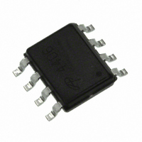
MOSFET P-CH -30V -9.7A 8-SOIC

AO4419

Manufacturer Part Number
AO4419
Description
MOSFET P-CH -30V -9.7A 8-SOIC
Manufacturer
Alpha & Omega Semiconductor Inc
Datasheet

Specifications of AO4419

Fet Type
MOSFET P-Channel, Metal Oxide
Fet Feature
Logic Level Gate
Rds On (max) @ Id, Vgs
20 mOhm @ 9.7A, 10V
Drain To Source Voltage (vdss)
30V
Current - Continuous Drain (id) @ 25° C
9.7A
Vgs(th) (max) @ Id
2.7V @ 250µA
Gate Charge (qg) @ Vgs
32nC @ 10V
Input Capacitance (ciss) @ Vds
1900pF @ 15V
Power - Max
3W
Mounting Type
Surface Mount
Package / Case
8-SOIC
Lead Free Status / RoHS Status
Lead free / RoHS Compliant
Other names
785-1024-2

Available stocks

Company
Part Number
Manufacturer
Quantity
Price
Part Number:
AO4419
Manufacturer:
AOS
Quantity:
90
Part Number:
AO4419
Manufacturer:
AO
Quantity:
40 000
Part Number:
AO4419
Manufacturer:
ALPHA
Quantity:
20 000
Company:
Part Number:
AO4419
Quantity:
30 000
Company:
Part Number:
AO4419
Quantity:
1 355
Company:
Part Number:
AO4419
Quantity:
560
Part Number:
AO4419**********
Manufacturer:
AOS全新
Quantity:
20 000
Part Number:
AO4419L
Manufacturer:
AOS/ 万代
Quantity:
20 000
Part Number:
AO4419L/
Manufacturer:
AOS/万代
Quantity:
20 000
Alpha & Omega Semiconductor, Ltd.
Absolute Maximum Ratings T
Parameter
Drain-Source Voltage
Gate-Source Voltage
Continuous Drain
Current
Pulsed Drain Current
Power Dissipation
Avalanche Current
Repetitive avalanche energy 0.1mH
Junction and Storage Temperature Range
Thermal Characteristics
Parameter
Maximum Junction-to-Ambient
Maximum Junction-to-Lead
General Description
The AO4419 uses advanced trench technology to
provide excellent R
device is suitable for use as a load switch or in PWM
applications.Standard Product AO4419 is
Pb-free (meets ROHS & Sony 259 specifications).
AO4419
P-Channel Enhancement Mode Field Effect Transistor
AF
S
S
S
G
A
B, G
DS(ON)
B
Top View
T
T
T
T
SOIC-8
A
A
A
A
=25°C
=70°C
=25°C
=70°C
, and low gate charge. This
C
AF
A
A
D
D
D
D
=25°C unless otherwise noted
B, G
Steady-State
Steady-State
t ≤ 10s
Symbol
V
V
I
I
P
I
E
T
D
DM
AR
DS
GS
D
AR
J
, T
STG
Symbol
Features
V
I
R
R
R
R
D
DS
DS(ON)
DS(ON)
θJA
θJL
= -9.7 A
(V) = -30V
< 20mΩ (V
< 35mΩ (V
Maximum
-55 to 150
G
±20
-9.7
-8.1
Typ
-30
-40
-30
2.1
45
31
63
21
3
(V
Rg,Ciss,Coss,Crss Tested
GS
D
S
GS
GS
= -10V)
= -10V)
= -4.5V)
Max
40
75
30
UIS TESTED!
www.aosmd.com
Units
Units
°C/W
°C/W
°C/W
mJ
°C
W
V
V
A
A

Related parts for AO4419

AO4419 Summary of contents

Page 1

... AO4419 P-Channel Enhancement Mode Field Effect Transistor General Description The AO4419 uses advanced trench technology to provide excellent R , and low gate charge. This DS(ON) device is suitable for use as a load switch or in PWM applications.Standard Product AO4419 is Pb-free (meets ROHS & Sony 259 specifications). ...

Page 2

... AO4419 Electrical Characteristics (T =25°C unless otherwise noted) J Symbol Parameter STATIC PARAMETERS BV Drain-Source Breakdown Voltage DSS I Zero Gate Voltage Drain Current DSS I Gate-Body leakage current GSS V Gate Threshold Voltage GS(th state drain current D(ON) R Static Drain-Source On-Resistance DS(ON) g Forward Transconductance FS V Diode Forward Voltage ...

Page 3

... AO4419 TYPICAL ELECTRICAL AND THERMAL CHARACTERISTICS 30 -10V - (Volts) DS Fig 1: On-Region Characteristics =-4. (A) D Figure 3: On-Resistance vs. Drain Current and Gate Voltage 25° (Volts) GS Figure 5: On-Resistance vs. Gate-Source Voltage Alpha & Omega Semiconductor, Ltd -3. =- 1.60 1.40 1.20 1.00 V =-10V GS 0. 1.0E+01 1.0E+00 I =-9.7A D 1.0E-01 1 ...

Page 4

... AO4419 TYPICAL ELECTRICAL AND THERMAL CHARACTERISTICS 10 V =-15V DS I =-9. (nC) g Figure 7: Gate-Charge Characteristics 100 In descending order T =25°C, 100°C, 125°C, 150° 0.001 0.01 0.1 Time in Avalache, t Figure 9: Single Pulse Avalanche Capability 0.001 0.01 Figure 11: Single Pulse Power Rating Junction-to-Ambient (Note E) Alpha & ...

Page 5

... AO4419 TYPICAL ELECTRICAL AND THERMAL CHARACTERISTICS 10 D =-15V =-9.7A θJA θJA J, =40°C/W θJA 1 0.1 0.01 Single Pulse 0.00001 0.0001 Alpha & Omega Semiconductor, Ltd. In descending order D=0.5, 0.3, 0.1, 0.05, 0.02, 0.01, single pulse 0.001 0.01 0.1 Pulse Width (s) Figure 12: Normalized Maximum Transient Thermal Impedance ...

Related keywords