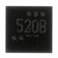
FDMA520PZ Fairchild Semiconductor, FDMA520PZ Datasheet - Page 2

FDMA520PZ
Manufacturer Part Number
FDMA520PZ
Description
MOSFET P-CH 20V 7.3A MLP2X2
Manufacturer
Fairchild Semiconductor
Series
PowerTrench®r
Datasheet
1.FDMA520PZ.pdf
(6 pages)
Specifications of FDMA520PZ
Fet Type
MOSFET P-Channel, Metal Oxide
Fet Feature
Logic Level Gate
Rds On (max) @ Id, Vgs
30 mOhm @ 7.3A, 4.5V
Drain To Source Voltage (vdss)
20V
Current - Continuous Drain (id) @ 25° C
7.3A
Vgs(th) (max) @ Id
1.5V @ 250µA
Gate Charge (qg) @ Vgs
20nC @ 4.5V
Input Capacitance (ciss) @ Vds
1645pF @ 10V
Power - Max
900mW
Mounting Type
Surface Mount
Package / Case
6-MLP, 6-MicroFET™
Transistor Polarity
P Channel
Continuous Drain Current Id
7.3A
Drain Source Voltage Vds
20V
On Resistance Rds(on)
30mohm
Rds(on) Test Voltage Vgs
12V
Threshold Voltage Vgs Typ
-1.1V
Rohs Compliant
Yes
Configuration
Single Quad Drain
Resistance Drain-source Rds (on)
30 mOhms
Forward Transconductance Gfs (max / Min)
22 S
Drain-source Breakdown Voltage
- 20 V
Gate-source Breakdown Voltage
+/- 12 V
Continuous Drain Current
7.3 A
Power Dissipation
2.4 W
Maximum Operating Temperature
+ 150 C
Mounting Style
SMD/SMT
Minimum Operating Temperature
- 55 C
Lead Free Status / RoHS Status
Lead free / RoHS Compliant
Other names
FDMA520PZTR
Available stocks
Company
Part Number
Manufacturer
Quantity
Price
Company:
Part Number:
FDMA520PZ
Manufacturer:
FSC
Quantity:
12 400
Part Number:
FDMA520PZ
Manufacturer:
FAIRCHILD/仙童
Quantity:
20 000
FDMA520PZ Rev.B2
Notes:
1: R
2: Pulse Test: Pulse Width < 300 s, Duty cycle < 2.0%.
3: The diode connected between the gate and the source serves only as protection against ESD. No gate overvoltage rating is implied.
Dynamic Characteristics
Electrical Characteristics
Off Characteristics
On Characteristics
Switching Characteristics
Drain-Source Diode Characteristics
BV
I
I
V
r
g
C
C
C
t
t
t
t
Q
Q
Q
I
V
t
Q
DSS
GSS
d(on)
r
d(off)
f
S
rr
DS(on)
FS
BV
GS(th)
SD
iss
oss
rss
g
gs
gd
rr
V
Symbol
DSS
T
T
GS(th)
JA
DSS
J
J
is the sum of the junction-to-case and case-to-ambient thermal resistance where the case thermal reference is defined as the solder mounting surface of the drain pins.
Drain to Source Breakdown Voltage
Breakdown Voltage Temperature
Coefficient
Zero Gate Voltage Drain Current
Gate to Source Leakage Current
Gate to Source Threshold Voltage
Gate to Source Threshold Voltage
Temperature Coefficient
Static Drain to Source On Resistance
Forward Transconductance
Input Capacitance
Output Capacitance
Reverse Transfer Capacitance
Turn-On Delay Time
Rise Time
Turn-Off Delay Time
Fall Time
Total Gate Charge
Gate to Source Gate Charge
Gate to Drain “Miller” Charge
Maximum Continuous Drain-Source Diode Forward Current
Source to Drain Diode Forward Voltage
Reverse Recovery Time
Reverse Recovery Charge
Parameter
a. 52°C/W when mounted on
a 1 in
2
pad of 2 oz copper
T
J
= 25°C unless otherwise noted
V
I
V
V
V
V
V
V
V
I
V
f = 1MHz
I
I
V
V
D
V
V
F
D
D
GS
GS
GS
GS
DS
GS
DD
GS
DS
DS
GS
DD
GS
=–7.3A, di/dt = 100A/ s
= –250 A, referenced to 25°C
= –250 A, V
= –250 A, referenced to 25°C
= –5V, I
= 0V, I
= V
= –4.5V, I
= –2.5V, I
= –4.5V, I
= –10V, V
= –10V, I
= –4.5V, R
= –16V, V
= ±12V, V
= –4.5V
= –5V, I
DS
2
Test Conditions
, I
S
D
D
= –2A
D
D
D
D
D
= –7.3A
= –250 A
GS
GS
DS
= –7.3A
GS
GEN
= –7.3A
= –7.3A
= –5.5A
= –7.3A ,T
= 0V
= 0V,
= 0V
= 0V
= 6
J
= 125°C
b.145°C/W when mounted on a
minimum pad of 2 oz copper
–0.6
Min
–20
–8.4
1235
–0.8
Typ
–1.1
255
225
2.9
4.4
22
3.5
10
29
83
74
14
30
26
42
36
22
Max
1645
–1.2
±10
–1.5
133
119
340
340
–1
20
47
20
–2
45
33
30
53
55
www.fairchildsemi.com
mV/°C
mV/°C
Units
m
nC
nC
nC
nC
pF
pF
pF
ns
ns
ns
ns
ns
V
V
S
A
V
A
A


