FDFMA2P029Z Fairchild Semiconductor, FDFMA2P029Z Datasheet

MOSFET P-CH 20V 3.1A 2X2MLP

FDFMA2P029Z

Manufacturer Part Number
FDFMA2P029Z
Description
MOSFET P-CH 20V 3.1A 2X2MLP
Manufacturer
Fairchild Semiconductor
Series
PowerTrench®r
Datasheet

Specifications of FDFMA2P029Z

Fet Type
MOSFET P-Channel, Metal Oxide
Fet Feature
Diode (Isolated)
Rds On (max) @ Id, Vgs
95 mOhm @ 3.1A, 4.5V
Drain To Source Voltage (vdss)
20V
Current - Continuous Drain (id) @ 25° C
3.1A
Vgs(th) (max) @ Id
1.5V @ 250µA
Gate Charge (qg) @ Vgs
10nC @ 4.5V
Input Capacitance (ciss) @ Vds
720pF @ 10V
Power - Max
700mW
Mounting Type
Surface Mount
Package / Case
6-MLP, 6-MicroFET™
Lead Free Status / RoHS Status
Lead free / RoHS Compliant
Other names
FDFMA2P029ZTR

Available stocks

Company
Part Number
Manufacturer
Quantity
Price
Part Number:
FDFMA2P029Z
Manufacturer:
Fairchild Semiconductor
Quantity:
41 800
©2008 Fairchild Semiconductor Corporation
FDFMA2P029Z Rev.B1
MOSFET Maximum Ratings
Thermal Characteristics
Package Marking and Ordering Information
FDFMA2P029Z
Integrated P-Channel PowerTrench
–20V, –3.1A, 95m:
Features
MOSFET
„ Max r
Schottky
„ V
„ Low profile - 0.8 mm maximum - in the new package
„ RoHS Compliant
V
V
I
P
T
V
I
R
R
R
R
D
O
J
DS
GS
D
RRM
TJA
TJA
TJA
TJA
HBM ESD protection level > 2.5kV (Note 3)
Max r
MicroFET 2x2 mm
, T
F
Symbol
Device Marking
STG
< 0.37V @ 500mA
DS(on)
DS(on)
.P29
= 95m: at V
= 141m: at V
Drain to Source Voltage
Gate to Source Voltage
Drain Current -Continuous
Power Dissipation
Operating and Storage Junction Temperature Range
Schottky Repetitive Peak Reverse Voltage
Schottky Average Forward Current
Thermal Resistance, Junction to Ambient
MicroFET 2X2
GS
GS
= –4.5V, I
FDFMA2P029Z
= –2.5V, I
-Pulsed
Device
D
D
= –3.1A
= –2.5A
T
C
A
= 25°C unless otherwise noted
Pin 1
A
Parameter
G
MicroFET 2X2
NC
Package
S
1
D
®
General Description
This device is designed specifically as a single package solution
for the battery charge switch in cellular handset and other ultra-
portable applications. It features a MOSFET with very low on-
state resistance and an independently connected low forward
voltage schottky diode allows for minimum conduction losses.
The MicroFET 2X2 package offers exceptional thermal
performance for its physical size and is well suited to linear mode
applications.
MOSFET and Schottky Diode
Reel Size
NC
7”
A
D
(Note 1a)
(Note 1b)
(Note 1d)
(Note 1a)
(Note 1a)
(Note 1b)
(Note 1c)
3
1
2
Tape Width
8mm
–55 to +150
Ratings
–3.1
–20
173
140
±12
1.4
0.7
20
86
86
-6
2
6
5
4
March 2008
www.fairchildsemi.com
S
C
G
Quantity
3000 units
Units
°C/W
°C
W
V
V
A
V
A

Related parts for FDFMA2P029Z

FDFMA2P029Z Summary of contents

Page 1

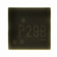
... Package Marking and Ordering Information Device Marking Device .P29 FDFMA2P029Z ©2008 Fairchild Semiconductor Corporation FDFMA2P029Z Rev.B1 ® MOSFET and Schottky Diode General Description This device is designed specifically as a single package solution for the battery charge switch in cellular handset and other ultra- = – ...

Page 2

... Maximum Continuous Drain-Source Diode Forward Current S V Source to Drain Diode Forward Voltage SD t Reverse Recovery Time rr Q Reverse Recovery Charge rr Schottky Diode Characteristics V Reverse Voltage R I Reverse Leakage R V Forward Voltage F FDFMA2P029Z Rev. 25°C unless otherwise noted J Test Conditions I = –250PA –250PA, referenced to 25° –16V ±12V ...

Page 3

... Pulse Test : Pulse Width < 300us, Duty Cycle < 2.0% 3. The diode connected between the gate and source serves only protection against ESD. No gate overvoltage rating is implied. FDFMA2P029Z Rev.B1 2 oz. copper pad on a 1.5 x 1.5 in. board of FR-4 material pad copper, 1.5" x 1.5" x 0.062" thick PCB 2 pad copper, 1.5” ...

Page 4

... T , JUNCTION TEMPERATURE J Figure 3. Normalized On-Resistance vs Junction Temperature 6 P PULSE DURATION = 300 s DUTY CYCLE = 2.0%MAX - 0.0 0.5 1 GATE TO SOURCE VOLTAGE (V) GS Figure 5. Transfer Characteristics FDFMA2P029Z Rev. 25°C unless otherwise noted -2. -1.5V GS 1.5 2.0 75 100 125 150 ( 125 0.001 ...

Page 5

... DS , DRAIN to SOURCE VOLTAGE (V) Figure 9. Forward Bias Safe Operating Area 125 0 0.001 0 200 400 V FORWARD VOLTAGE(mV) F, Figure 11. Schottky Diode Forward Voltage FDFMA2P029Z Rev. 25°C unless otherwise noted J 1000 = - -15V -10V 100us 1ms 10ms 100ms 1s 10s 0.01 0.001 600 800 Figure 12 ...

Page 6

... Typical Characteristics 2 1 DUTY CYCLE-DESCENDING ORDER D = 0.5 0.2 0.1 0.05 0.1 0.02 0.01 SINGLE PULSE 0.01 0.005 - FDFMA2P029Z Rev. 25°C unless otherwise noted RECTANGULAR PULSE DURATION (s) Figure 13. Transient Thermal Response Curve NOTES: DUTY FACTOR PEAK TJA TJA www.fairchildsemi.com 3 10 ...

Page 7

... Dimensional Outline and Pad Layout rev3 FDFMA2P029Z Rev.B1 7 www.fairchildsemi.com ...

Page 8

... Definition of Terms Datasheet Identification Product Status Advance Information Formative or In Design Preliminary First Production No Identification Needed Full Production Obsolete Not In Production FDFMA2P029Z Rev.B1 FPS™ PDP-SPM™ F-PFS™ Power-SPM™ ® FRFET PowerTrench SM Global Power Resource Programmable Active Droop™ ...

Related keywords