FDT434P Fairchild Semiconductor, FDT434P Datasheet
FDT434P
Specifications of FDT434P
Available stocks


Related parts for FDT434P


FDT434P Summary of contents
Page 1
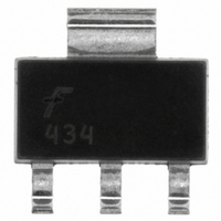
... R θJC Package Marking and Ordering Information Device Marking Device 434 FDT434P ©2011 Fairchild Semiconductor Corporation FDT434P Rev. C2 MOSFET Features • –5.5 A, – advanced • Low gate charge (13nC typical) • High performance trench technology for extremely low R • ...
Page 2
... R is guaranteed by design while R θJC a) 42°C/W when mounted on a 1in pad copper Scale letter size paper 2. Pulse Test: Pulse Width < 300µs, Duty Cycle < 2.0% ©2011 Fairchild Semiconductor Corporation FDT434P Rev 25°C unless otherwise noted A Test Conditions = –250 µ – ...
Page 3
... Figure 3. On-Resistance Variation withTemperature - -55° 0.9 1.2 1.5 1 GATE TO SOURCE VOLTAGE (V) GS Figure 5. Transfer Characteristics. ©2011 Fairchild Semiconductor Corporation FDT434P Rev. C2 1.8 1 1.4 -2.0V 1.2 1 -1 Figure 2. On-Resistance Variation with Drain Current and Gate Voltage. 0.15 0.12 0.09 0.06 0.03 ...
Page 4
... DS Figure 9. Maximum Safe Operating Area 0.5 0.2 0.1 0.1 0.05 0.02 0.01 0.01 Single Pulse 0.001 0.001 0.01 Figure 11. Transient Thermal Response Curve. ©2011 Fairchild Semiconductor Corporation FDT434P Rev. C2 1800 1600 = -5V -10V 1400 -15V 1200 1000 800 600 400 200 Figure 8. Capacitance Characteristics. ...
Page 5
... Datasheet Identification Product Status Advance Information Formative / In Design Preliminary First Production No Identification Needed Full Production Obsolete Not In Production ©2011 Fairchild Semiconductor Corporation FDT434P Rev. C2 Power-SPM™ ® PowerTrench SM PowerXS™ Programmable Active Droop™ ® QFET QS™ Quiet Series™ RapidConfigure™ ...