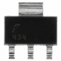
FDT434P Fairchild Semiconductor, FDT434P Datasheet - Page 4

FDT434P
Manufacturer Part Number
FDT434P
Description
MOSFET P-CH 20V 6A SOT-223
Manufacturer
Fairchild Semiconductor
Series
PowerTrench®r
Type
Power MOSFETr
Specifications of FDT434P
Fet Type
MOSFET P-Channel, Metal Oxide
Fet Feature
Logic Level Gate
Rds On (max) @ Id, Vgs
50 mOhm @ 6A, 4.5V
Drain To Source Voltage (vdss)
20V
Current - Continuous Drain (id) @ 25° C
6A
Vgs(th) (max) @ Id
1V @ 250µA
Gate Charge (qg) @ Vgs
19nC @ 4.5V
Input Capacitance (ciss) @ Vds
1187pF @ 10V
Power - Max
1.1W
Mounting Type
Surface Mount
Package / Case
SOT-223 (3 leads + Tab), SC-73, TO-261
Configuration
Single Dual Drain
Transistor Polarity
P-Channel
Resistance Drain-source Rds (on)
0.05 Ohm @ 4.5 V
Forward Transconductance Gfs (max / Min)
6.5 S
Drain-source Breakdown Voltage
20 V
Gate-source Breakdown Voltage
+/- 8 V
Continuous Drain Current
6 A
Power Dissipation
3000 mW
Maximum Operating Temperature
+ 150 C
Mounting Style
SMD/SMT
Minimum Operating Temperature
- 55 C
Number Of Elements
1
Polarity
P
Channel Mode
Enhancement
Drain-source On-res
0.05Ohm
Drain-source On-volt
20V
Gate-source Voltage (max)
±8V
Drain Current (max)
6A
Output Power (max)
Not RequiredW
Frequency (max)
Not RequiredMHz
Noise Figure
Not RequireddB
Power Gain
Not RequireddB
Drain Efficiency
Not Required%
Operating Temp Range
-55C to 150C
Operating Temperature Classification
Military
Mounting
Surface Mount
Pin Count
3 +Tab
Package Type
SOT-223
Continuous Drain Current Id
6A
Drain Source Voltage Vds
-20V
On Resistance Rds(on)
40mohm
Rds(on) Test Voltage Vgs
-4.5V
Threshold Voltage Vgs Typ
-600mV
Transistor Case Style
SOT-223
Rohs Compliant
Yes
Lead Free Status / RoHS Status
Lead free / RoHS Compliant
Other names
FDT434P
Available stocks
Company
Part Number
Manufacturer
Quantity
Price
Company:
Part Number:
FDT434P
Manufacturer:
FSC
Quantity:
35 000
Part Number:
FDT434P
Manufacturer:
FAIRCHILD/仙童
Quantity:
20 000
©2011 Fairchild Semiconductor Corporation
FDT434P Rev. C2
Typical Characteristics
5
4
3
2
1
0
0
0.01
100
0.1
Figure 9. Maximum Safe Operating Area.
10
I
1
Figure 7. Gate Charge Characteristics.
0.001
D
0.1
0.01
0.1
= -6.0A
1
0.001
R
SINGLE PULSE
DS(ON)
R
V
θJA
T
GS
= 110
A
3
= -4.5V
= 25
LIMIT
D = 0.5
o
o
C/W
C
-V
0.2
0.05
0.02
0.1
0.01
Q
DS
Single Pulse
, DRAIN-SOURCE VOLTAGE (V)
g
, GATE CHARGE (nC)
1
6
0.01
DC
10s
V
Figure 11. Transient Thermal Response Curve.
DS
1s
9
= -5V
Thermal characterization performed using the conditions described in Note 1c.
Transient thermal response will change depending on the circuit board design.
100ms
10ms
-10V
10
-15V
100 µ s
12
0.1
15
100
t
1
, TIME (sec)
4
1
200
160
120
1800
1600
1400
1200
1000
80
40
800
600
400
200
0.0001
0
Figure 8. Capacitance Characteristics.
0
0
Figure 10. Single Pulse Maximum
0.001
2
C
Power Dissipation.
-V
RSS
10
DS
0.01
, DRAIN TO SOURCE VOLTAGE (V)
SINGLE PULSE TIME (SEC)
4
C
0.1
OSS
6
1
P(pk)
Duty Cycle, D = t
C
T
R
100
ISS
R
J
θJA
- T
θJA
8
(t) = r(t) * R
A
10
= 110 °C/W
t
1
SINGLE PULSE
R
www.fairchildsemi.com
= P * R
t
2
θ JA
T
V
f = 1MHz
A
= 110
GS
= 25
10
100
= 0 V
θJA
o
o
1
θJA
C
C/W
(t)
/ t
2
1000
1000
12


