RFP50N06 Fairchild Semiconductor, RFP50N06 Datasheet
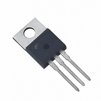
MOSFET N-CH 60V 50A TO-220AB

RFP50N06

Manufacturer Part Number
RFP50N06
Description
MOSFET N-CH 60V 50A TO-220AB
Manufacturer
Fairchild Semiconductor
Datasheet

Specifications of RFP50N06

Fet Type
MOSFET N-Channel, Metal Oxide
Fet Feature
Standard
Rds On (max) @ Id, Vgs
22 mOhm @ 50A, 10V
Drain To Source Voltage (vdss)
60V
Current - Continuous Drain (id) @ 25° C
50A
Vgs(th) (max) @ Id
4V @ 250µA
Gate Charge (qg) @ Vgs
150nC @ 20V
Input Capacitance (ciss) @ Vds
2020pF @ 25V
Power - Max
131W
Mounting Type
Through Hole
Package / Case
TO-220-3 (Straight Leads)
Configuration
Single
Transistor Polarity
N-Channel
Resistance Drain-source Rds (on)
0.022 Ohm @ 10 V
Drain-source Breakdown Voltage
60 V
Gate-source Breakdown Voltage
+/- 20 V
Continuous Drain Current
50 A
Power Dissipation
131000 mW
Maximum Operating Temperature
+ 175 C
Mounting Style
Through Hole
Minimum Operating Temperature
- 55 C
Lead Free Status / RoHS Status
Lead free / RoHS Compliant

Available stocks

Company
Part Number
Manufacturer
Quantity
Price
Part Number:
RFP50N06
Manufacturer:
FSC
Quantity:
44 920
Part Number:
RFP50N06
Manufacturer:
FAIRCHILD
Quantity:
3 690
Part Number:
RFP50N06
Manufacturer:
ST
Quantity:
20 000
Part Number:
RFP50N06
Manufacturer:
FAIRCHILD/仙童
Quantity:
20 000
Company:
Part Number:
RFP50N06
Quantity:
2 500
Company:
Part Number:
RFP50N06
Quantity:
15 087
Part Number:
RFP50N06LE
Manufacturer:
KA/INTRISII
Quantity:
12 500
©2002 Fairchild Semiconductor Corporation
50A, 60V, 0.022 Ohm, N-Channel Power
MOSFETs
These N-Channel power MOSFETs are manufactured using
the MegaFET process. This process, which uses feature
sizes approaching those of LSI integrated circuits gives
optimum utilization of silicon, resulting in outstanding
performance. They were designed for use in applications
such as switching regulators, switching converters, motor
drivers, and relay drivers. These transistors can be operated
directly from integrated circuits.
Formerly developmental type TA49018.
Ordering Information
NOTE: When ordering, use the entire part number. Add the suffix, 9A,
to obtain the TO-263AB variant in tape and reel, i.e. RF1S50N06SM9A.
Packaging
RFG50N06
RFP50N06
RF1S50N06SM
PART NUMBER
SIDE METAL)
(BOTTOM
DRAIN
JEDEC STYLE TO-247
TO-247
TO-220AB
TO-263AB
PACKAGE
Data Sheet
RFP50N06
F1S50N06
RFG50N06
SOURCE
DRAIN
BRAND
SOURCE
GATE
GATE
RFG50N06, RFP50N06, RF1S50N06SM
JEDEC TO-263AB
Features
• 50A, 60V
• r
• Temperature Compensating PSPICE
• Peak Current vs Pulse Width Curve
• UIS Rating Curve
• 175
Symbol
DS(ON)
(FLANGE)
DRAIN
o
C Operating Temperature
January 2002
(FLANGE)
= 0.022 Ω
DRAIN
JEDEC TO-220AB
G
RFG50N06, RFP50N06, RF1S50N06SM Rev. B
D
S
®
SOURCE
Model
DRAIN
GATE

Related parts for RFP50N06

RFP50N06 Summary of contents

Page 1

... Peak Current vs Pulse Width Curve • UIS Rating Curve o • 175 C Operating Temperature Symbol BRAND RFG50N06 RFP50N06 F1S50N06 SOURCE DRAIN GATE JEDEC TO-263AB GATE DRAIN (FLANGE) SOURCE January 2002 = 0.022 Ω ® Model JEDEC TO-220AB SOURCE DRAIN GATE DRAIN (FLANGE) RFG50N06, RFP50N06, RF1S50N06SM Rev. B ...

Page 2

... L 260 MIN TYP 150 48V 50A, - 125 0.96 Ω 1.45mA g(REF) - 3.7 - 2020 - 600 - 200 - - - - - - MIN TYP - - - - RFG50N06, RFP50N06, RF1S50N06SM Rev. B UNITS MAX UNITS - µ µ ± 100 nA Ω 0.022 150 4 1. C/W MAX UNITS 1.5 V 125 ns ...

Page 3

... FOR TEMPERATURES ABOVE 25 DERATE PEAK CURRENT CAPABILITY AS FOLLOWS:  20V   10V GS 2 TRANSCONDUCTANCE MAY LIMIT CURRENT IN THIS REGION PULSE WIDTH (ms) FIGURE 5. PEAK CURRENT CAPABILITY RFG50N06, RFP50N06, RF1S50N06SM Rev. B 125 150 175 θJC θ 175 T C –   ----------------------- - 150  ...

Page 4

... DUTY CYCLE = 0.5% MAX V = 10V 50A GS D 2.0 1.5 1.0 0.5 0 -80 - JUNCTION TEMPERATURE ( J RESISTANCE vs JUNCTION TEMPERATURE 2 250µA D 1.5 1.0 0.5 0 -80 - JUNCTION TEMPERATURE ( J VOLTAGE vs JUNCTION TEMPERATURE RFG50N06, RFP50N06, RF1S50N06SM Rev 6.0 7.5 120 160 200 o C) 120 160 200 o C) ...

Page 5

... DSS DSS R = 1.2Ω 1.45mA g(REF 10V GS I g(REF TIME (µ g(ACT) CONSTANT GATE CURRENT BV DSS FIGURE 15. UNCLAMPED ENERGY WAVEFORMS d(ON) d(OFF 90% 10% 50% PULSE WIDTH FIGURE 17. SWITCHING WAVEFORMS RFG50N06, RFP50N06, RF1S50N06SM Rev DSS 7.5 5.0 2 g(REF) I g(ACT OFF t f 90% 10% 90% 50% ...

Page 6

... Test Circuits and Waveforms g(REF) FIGURE 18. GATE CHARGE TEST CIRCUIT ©2002 Fairchild Semiconductor Corporation (Continued DUT g(REF g(TOT g(10 10V GS Q g(TH) FIGURE 19. GATE CHARGE WAVEFORMS RFG50N06, RFP50N06, RF1S50N06SM Rev 20V GS ...

Page 7

... Options; authors, William J. Hepp and C. Frank Wheatley. ©2002 Fairchild Semiconductor Corporation 10 DPLCAP - 6 ESG EVTO GATE - LGATE RGATE RIN S1A S2A S1B S2B EGS LDRAIN RDRAIN DBREAK 16 VTO DBODY MOS2 MOS1 17 EBREAK 18 - CIN RSOURCE LSOURCE 7 8 RBREAK EDS 8 - RFG50N06, RFP50N06, RF1S50N06SM Rev. B DRAIN 2 3 SOURCE 18 RVTO 19 - VBAT + ...

Page 8

... TRADEMARKS The following are registered and unregistered trademarks Fairchild Semiconductor owns or is authorized to use and is not intended exhaustive list of all such trademarks. ACEx™ FAST Bottomless™ FASTr™ FRFET™ CoolFET™ GlobalOptoisolator™ CROSSVOLT™ GTO™ DenseTrench™ ...

Related keywords