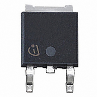
SPD35N10 Infineon Technologies, SPD35N10 Datasheet - Page 2

SPD35N10
Manufacturer Part Number
SPD35N10
Description
MOSFET N-CH 100V 35A DPAK
Manufacturer
Infineon Technologies
Series
SIPMOS®r
Datasheet
1.SPD35N10.pdf
(8 pages)
Specifications of SPD35N10
Fet Type
MOSFET N-Channel, Metal Oxide
Fet Feature
Standard
Rds On (max) @ Id, Vgs
44 mOhm @ 26.4A, 10V
Drain To Source Voltage (vdss)
100V
Current - Continuous Drain (id) @ 25° C
35A
Gate Charge (qg) @ Vgs
65nC @ 10V
Input Capacitance (ciss) @ Vds
1570pF @ 25V
Power - Max
150W
Mounting Type
Surface Mount
Package / Case
DPak, TO-252 (2 leads+tab), SC-63
Lead Free Status / RoHS Status
Lead free / RoHS Compliant
Vgs(th) (max) @ Id
-
Other names
SP000013853
SPD35N10INTR
SPD35N10XT
SPD35N10XTINTR
SPD35N10XTINTR
SPD35N10INTR
SPD35N10XT
SPD35N10XTINTR
SPD35N10XTINTR
Available stocks
Company
Part Number
Manufacturer
Quantity
Price
Company:
Part Number:
SPD35N10
Manufacturer:
AD
Quantity:
2 300
1 Device on 40mm*40mm*1.5mm epoxy PCB FR4 with 6cm² (one layer, 70 µm thick) copper area for drain
connection. PCB is vertical without blown air.
Electrical Characteristics, at T
Parameter
Static Characteristics
Drain-source breakdown voltage
V
Gate threshold voltage, V
I
Zero gate voltage drain current
V
V
Gate-source leakage current
V
Drain-source on-state resistance
V
Thermal Characteristics
Parameter
Characteristics
Thermal resistance, junction - case
Thermal resistance, junction - ambient, leaded
SMD version, device on PCB:
@ min. footprint
@ 6 cm
D
GS
DS
DS
GS
GS
= - µA
=100V, V
=100V, V
=0V, I
=20V, V
=10V, I
2
cooling area
D
D
=1mA
DS
=26.4A
GS
GS
=0V
=0V, T
=0V, T
F)
j
j
=25°C
=125°C
GS
= V
j
DS
= 25 °C, unless otherwise specified
Preliminary data
Page 2
Symbol
V
V
I
I
R
Symbol
R
R
R
DSS
GSS
(BR)DSS
GS(th)
DS(on)
thJC
thJA
thJA
min.
min.
100
2.1
-
-
-
-
-
-
-
-
Values
Values
0.01
typ.
typ.
36
3
1
1
-
-
-
-
-
max.
max.
100
100
100
SPD35N10
44
75
50
2002-01-30
4
1
1
-
Unit
V
µA
nA
m
Unit
K/W


