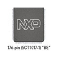
LH79520N0M000B1 NXP Semiconductors, LH79520N0M000B1 Datasheet - Page 50

LH79520N0M000B1
Manufacturer Part Number
LH79520N0M000B1
Description
Manufacturer
NXP Semiconductors
Datasheet
1.LH79520N0M000B1.pdf
(59 pages)
Specifications of LH79520N0M000B1
Operating Temperature (min)
-40C
Operating Temperature (max)
85C
Processing Unit
Microcontroller
Operating Supply Voltage (min)
1.62V
Operating Supply Voltage (typ)
1.8V
Operating Supply Voltage (max)
1.98V
Package Type
LQFP
Screening Level
Industrial
Pin Count
176
Mounting
Surface Mount
Rad Hardened
No
Lead Free Status / RoHS Status
Not Compliant
Available stocks
Company
Part Number
Manufacturer
Quantity
Price
Company:
Part Number:
LH79520N0M000B1
Manufacturer:
Sharp Microelectronics
Quantity:
10 000
LH79520
Printed Circuit Board Layout Practices
LH79520 POWER SUPPLY DECOUPLING
for different internal circuitry sections. The VDD and
VSS pins supply power to I/O buffers, while VDDC and
VSSC supply power to the core logic.
with a low impedance path to the corresponding board
power supply. Likewise, the VSS and VSSC pins must be
provided with a low impedance path to the board ground.
using at least one 0.1 µF high frequency capacitor
located as close as possible to a VDDx, VSSx pin pair
on each of the four sides of the chip. If room on the cir-
cuit board allows, add one 0.01 µF high frequency
capacitor near each VDDx, VSSx pair on the chip.
circuit board traces connecting to the chip VDDx, VSSx
pins must be kept to less than half an inch (12.7 mm)
per capacitor lead. There must be one bulk 10 µF
capacitor for each power supply placed near one side
of the chip.
REQUIRED LH79520 PLL, VDDA, VSSA FILTER
cuitry. VSSA is the ground return path for the PLL circuit.
If the internal PLL circuit will be used, these pins must
have a low-pass filter attached as shown in Figure 32.
have a low forward drop specification, to allow VDDA to
quickly transition through the entire input voltage range.
from the IC package pin to the high frequency capaci-
tor, then to the low frequency capacitor, and finally
through the series resistor to the board power supply.
The distance from the IC pin to the high frequency
capacitor must be kept as short as possible.
50
(SOURCE)
The LH79520 has separate power and ground pins
Each of the VDD and VDDC pins must be provided
Each power supply must be decoupled to ground
To be effective, the capacitor leads and associated
The VDDA pin supplies power to the chip PLL cir-
The Schottky diode shown in the schematic must
The power pin VDDA path must be a single wire
VDDC
Figure 32. VDDA, VSSA Filter Circuit
100 Ω
22 µF
+
PIN 92
0.1 µF
PIN 91
VSSA
VDDC
VDDA
LH79520
Rev. 01 — 16 July 2007
NXP Semiconductors
79520-64
high frequency capacitor, then to the low frequency
capacitor, keeping the distance from the IC pin to the
high frequency cap as short as possible.
Note that the VSSA pin specifically does not have a connection to the
circuit board ground. The LH79520 PLL circuit has an internal DC
ground connection to VSS (GND), so the external VSSA pin must
NOT be connected to the circuit board ground, but only to the filter
components.
UNUSED INPUT SIGNAL CONDITIONING
consumption. Unused inputs which do not include inter-
nal pull-up or pull-down resistors should be pulled up or
down externally, to tie the signal to its inactive state.
which carry these signals are unused, software can
program these signals as outputs, to eliminate the need
for pull-ups or pull-downs. Power consumption may be
higher than expected until such software executes.
downs. If unused, these inputs do not require external
conditioning.
OTHER CIRCUIT BOARD LAYOUT PRACTICES
times. Printed circuit trace interconnection length must
therefore be reduced to minimize overshoot, under-
shoot and reflections caused by transmission line
effects of these fast output switching times. This rec-
ommendation particularly applies to the address and
data buses.
consider all device loads and capacitances due to the
circuit board traces. Capacitance due to the traces will
depend upon a number of factors, including the trace
width, dielectric material the circuit board is made from
and proximity to ground and power planes.
cuit board layout becomes more critical in systems with
higher capacitive loads. As these capacitive loads
increase, transient currents in the power supply and
ground return paths also increase.
an internal pull-down resistor has been specified;
see Table 3. (All pull-up/pull-down resistors must be
33 KΩ MAX.) Consider all signals that are Inputs at
Reset time.
Similarly, the VSSA path is from the IC pin to the
Floating input signals can cause excessive power
Some GPIO signals may default to inputs. If the pins
Some LH79520 inputs have internal pull-ups or pull-
All output pins on the LH79520 have fast rise and fall
When considering capacitance, calculations must
Attention to power supply decoupling and printed cir-
Add pull-up resistors to all unused inputs unless
CAUTION
Preliminary data sheet
System-on-Chip


