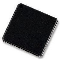
ADSP-BF592KCPZ Analog Devices Inc, ADSP-BF592KCPZ Datasheet - Page 12

ADSP-BF592KCPZ
Manufacturer Part Number
ADSP-BF592KCPZ
Description
58T4522
Manufacturer
Analog Devices Inc
Specifications of ADSP-BF592KCPZ
Operating Temperature (min)
0C
Operating Temperature (max)
70C
Operating Temperature Classification
Commercial
Mounting
Surface Mount
Pin Count
64
Rohs Compliant
YES
Frequency
400MHz
Embedded Interface Type
PPI, SPI, UART
No. Of I/o's
32
Operating Temperature Range
0°C To +70°C
Digital Ic Case Style
LFCSP
No. Of Pins
64
Core Supply Voltage
1.4V
Lead Free Status / RoHS Status
Compliant
Available stocks
Company
Part Number
Manufacturer
Quantity
Price
Company:
Part Number:
ADSP-BF592KCPZ-2
Manufacturer:
BROADCOM
Quantity:
154
ADSP-BF592
VOLTAGE REGULATION
The ADSP-BF592 processor requires an external voltage regula-
tor to power the V
consumption, the external voltage regulator can be signaled
through EXT_WAKE to remove power from the processor core.
This signal is high-true for power-up and may be connected
directly to the low-true shut-down input of many common
regulators.
While in the hibernate state, the external supply, V
still be applied, eliminating the need for external buffers. The
external voltage regulator can be activated from this power
down state by asserting the RESET pin, which then initiates a
boot sequence. EXT_WAKE indicates a wakeup to the external
voltage regulator.
The power good (PG) input signal allows the processor to start
only after the internal voltage has reached a chosen level. In this
way, the startup time of the external regulator is detected after
hibernation. For a complete description of the power good
functionality, refer to the ADSP-BF59x Blackfin Processor Hard-
ware Reference.
CLOCK SIGNALS
The processor can be clocked by an external crystal, a sine wave
input, or a buffered, shaped clock derived from an external
clock oscillator.
If an external clock is used, it should be a TTL-compatible signal
and must not be halted, changed, or operated below the speci-
fied frequency during normal operation. This signal is
connected to the processor’s CLKIN pin. When an external
clock is used, the XTAL pin must be left unconnected.
Alternatively, because the processor includes an on-chip oscilla-
tor circuit, an external crystal may be used. For fundamental
frequency operation, use the circuit shown in
lel-resonant, fundamental frequency, microprocessor-grade
crystal is connected across the CLKIN and XTAL pins. The on-
chip resistance between CLKIN and the XTAL pin is in the
500 kΩ range. Further parallel resistors are typically not recom-
mended. The two capacitors and the series resistor shown in
Figure 4
The capacitor and resistor values shown in
values only. The capacitor values are dependent upon the crystal
manufacturers’ load capacitance recommendations and the PCB
physical layout. The resistor value depends on the drive level
f
V
V
T
T
CCLKRED
NOM
RED
DDINTNOM
DDINTRED
is the duration running at f
is the duration running at f
fine tune phase and amplitude of the sine frequency.
is the reduced core clock frequency
is the reduced internal supply voltage
is the nominal internal supply voltage
DDINT
domain. To reduce standby power
CCLKRED
CCLKNOM
Figure 4
Figure
Rev. PrC | Page 12 of 46 | August 2010
DDEXT
are typical
4. A paral-
, can
specified by the crystal manufacturer. The user should verify the
customized values based on careful investigations on multiple
devices over temperature range.
A third-overtone crystal can be used for frequencies above 25
MHz. The circuit is then modified to ensure crystal operation
only at the third overtone, by adding a tuned inductor circuit as
shown in
ation is discussed in detail in application note (EE-168) Using
Third Overtone Crystals with the ADSP-218x DSP on the Analog
Devices website (www.analog.com)—use site search on
“EE-168.”
The Blackfin core runs at a different clock rate than the on-chip
peripherals. As shown in
system peripheral clock (SCLK) are derived from the input
clock (CLKIN) signal. An on-chip PLL is capable of multiplying
the CLKIN signal by a programmable 5× to 64× multiplication
factor (bounded by specified minimum and maximum VCO
frequencies). The default multiplier is 6×, but it can be modified
by a software instruction sequence.
On-the-fly frequency changes can be effected by simply writing
to the PLL_DIV register. The maximum allowed CCLK and
SCLK rates depend on the applied voltages V
the VCO is always permitted to run up to the frequency speci-
fied by the part’s instruction rate. The CLKOUT pin reflects the
SCLK frequency to the off-chip world. The pin functions as a
reference signal in many timing specifications. While three-
stated by default, it can be enabled using the VRCTL register.
All on-chip peripherals are clocked by the system clock (SCLK).
The system clock frequency is programmable by means of the
SSEL3–0 bits of the PLL_DIV register. The values programmed
into the SSEL fields define a divide ratio between the PLL output
(VCO) and the system clock. SCLK divider values are 1 through
15.
Table 6
EXTCLK
NOTE: VALUES MARKED WITH * MUST BE CUSTOMIZED, DEPENDING
ON THE CRYSTAL AND LAYOUT. PLEASE ANALYZE CAREFULLY. FOR
FREQUENCIES ABOVE 33 MHz, THE SUGGESTED CAPACITOR VALUE
OF 18 pF SHOULD BE TREATED AS A MAXIMUM, AND THE SUGGESTED
RESISTOR VALUE SHOULD BE REDUCED TO 0
EN
Figure
illustrates typical system clock ratios.
SELECT
Figure 4. External Crystal Connections
4. A design procedure for third-overtone oper-
EN
Preliminary Technical Data
BLACKFIN
CLKBUF
CLKIN
Figure
18 pF *
330
TO PLL CIRCUITRY
5, the core clock (CCLK) and
CLKOUT (SCLK)
*
560
XTAL
18 pF *
.
FOR OVERTONE
OPERATION ONLY:
DDINT
and V
DDEXT
;


