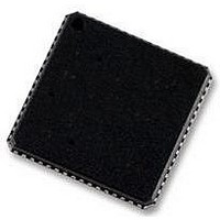
ADSP-BF592KCPZ Analog Devices Inc, ADSP-BF592KCPZ Datasheet - Page 4

ADSP-BF592KCPZ
Manufacturer Part Number
ADSP-BF592KCPZ
Description
58T4522
Manufacturer
Analog Devices Inc
Specifications of ADSP-BF592KCPZ
Operating Temperature (min)
0C
Operating Temperature (max)
70C
Operating Temperature Classification
Commercial
Mounting
Surface Mount
Pin Count
64
Rohs Compliant
YES
Frequency
400MHz
Embedded Interface Type
PPI, SPI, UART
No. Of I/o's
32
Operating Temperature Range
0°C To +70°C
Digital Ic Case Style
LFCSP
No. Of Pins
64
Core Supply Voltage
1.4V
Lead Free Status / RoHS Status
Compliant
Available stocks
Company
Part Number
Manufacturer
Quantity
Price
Company:
Part Number:
ADSP-BF592KCPZ-2
Manufacturer:
BROADCOM
Quantity:
154
ADSP-BF592
population count, modulo 2
ration and rounding, and sign/exponent detection. The set of
video instructions include byte alignment and packing opera-
tions, 16-bit and 8-bit adds with clipping, 8-bit average
operations, and 8-bit subtract/absolute value/accumulate (SAA)
operations. Also provided are the compare/select and vector
search instructions.
For certain instructions, two 16-bit ALU operations can be per-
formed simultaneously on register pairs (a 16-bit high half and
16-bit low half of a compute register). If the second ALU is used,
quad 16-bit operations are possible.
The 40-bit shifter can perform shifts and rotates and is used to
support normalization, field extract, and field deposit
instructions.
The program sequencer controls the flow of instruction execu-
tion, including instruction alignment and decoding. For
program flow control, the sequencer supports PC relative and
indirect conditional jumps (with static branch prediction), and
subroutine calls. Hardware is provided to support zero-over-
head looping. The architecture is fully interlocked, meaning that
the programmer need not manage the pipeline when executing
instructions with data dependencies.
DA1
DA0
LD1
LD0
SD
32
32
32
32
32
32
R1.H
R0.H
R7.H
R6.H
R3.H
R2.H
R5.H
R4.H
multiply, divide primitives, satu-
RAB
32
R0.L
R7.L
R2.L
R1.L
I3
R6.L
R5.L
R4.L
R3.L
I2
I1
I0
32
L3
L2
L1
L0
32
SHIFTER
BARREL
B3
B2
B1
B0
8
Rev. PrC | Page 4 of 46 | August 2010
ADDRESS ARITHMETIC UNIT
32
M3
M2
Figure 2. Blackfin Processor Core
M1
M0
A0
DATA ARITHMETIC UNIT
16
40
32
DAG1
8
40
40
The address arithmetic unit provides two addresses for simulta-
neous dual fetches from memory. It contains a multiported
register file consisting of four sets of 32-bit index, modify,
length, and base registers (for circular buffering), and eight
additional 32-bit pointer registers (for C-style indexed stack
manipulation).
Blackfin processors support a modified Harvard architecture in
combination with a hierarchical memory structure. Level 1 (L1)
memories are those that typically operate at the full processor
speed with little or no latency. At the L1 level, the instruction
memory holds instructions only. Data memory holds data, and
a dedicated scratchpad data memory stores stack and local vari-
able information.
Multiple L1 memory blocks are provided. The memory man-
agement unit (MMU) provides memory protection for
individual tasks that may be operating on the core and can pro-
tect system registers from unintended access.
The architecture provides three modes of operation: user mode,
supervisor mode, and emulation mode. User mode has
restricted access to certain system resources, thus providing a
protected software environment, while supervisor mode has
unrestricted access to the system and core resources.
8
DAG0
16
40
A1
ASTAT
P2
P1
P0
SP
FP
P5
P4
P3
Preliminary Technical Data
8
32
PREG
LOOP BUFFER
SEQUENCER
DECODE
CONTROL
ALIGN
UNIT


