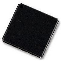
ADSP-BF592KCPZ Analog Devices Inc, ADSP-BF592KCPZ Datasheet - Page 16

ADSP-BF592KCPZ
Manufacturer Part Number
ADSP-BF592KCPZ
Description
58T4522
Manufacturer
Analog Devices Inc
Specifications of ADSP-BF592KCPZ
Operating Temperature (min)
0C
Operating Temperature (max)
70C
Operating Temperature Classification
Commercial
Mounting
Surface Mount
Pin Count
64
Rohs Compliant
YES
Frequency
400MHz
Embedded Interface Type
PPI, SPI, UART
No. Of I/o's
32
Operating Temperature Range
0°C To +70°C
Digital Ic Case Style
LFCSP
No. Of Pins
64
Core Supply Voltage
1.4V
Lead Free Status / RoHS Status
Compliant
Available stocks
Company
Part Number
Manufacturer
Quantity
Price
Company:
Part Number:
ADSP-BF592KCPZ-2
Manufacturer:
BROADCOM
Quantity:
154
ADSP-BF592
SIGNAL DESCRIPTIONS
Signal definitions for the ADSP-BF592 processor are listed in
Table
package size and pin count, some pins have dual, multiplexed
functions. In cases where pin function is reconfigurable, the
default state is shown in plain text, while the alternate function
is shown in italics.
All pins are three-stated during and immediately after reset,
with the exception of EXT_CLK, which toggles at the system
clock rate.
Table 9. Signal Descriptions
Signal Name
Port F: GPIO and Multiplexed Peripherals
Port G: GPIO and Multiplexed Peripherals
PF0–GPIO/DR1SEC/PPI_D8/WAKEN1
PF1–GPIO/DR1PRI/PPI_D9
PF2–GPIO/RSCLK1/PPI_D10
PF3–GPIO/RFS1/PPI_D11
PF4–GPIO/DT1SEC/PPI_D12
PF5–GPIO/DT1PRI/PPI_D13
PF6–GPIO/TSCLK1/PPI_D14
PF7–GPIO/TFS1/PPI_D15
PF8–GPIO/TMR2/SPI0_SSEL2/WAKEN0
PF9–GPIO/TMR0/PPI_FS1/SPI0_SSEL3
PF10–GPIO/TMR1/PPI_FS2
PF11–GPIO/UA_TX/SPI0_SSEL4
PF12–GPIO/UA_RX/SPI0_SSEL7/TACI2–0
PF13–GPIO/SPI0_MOSI/SPI1_SSEL3
PF14–GPIO/SPI0_MISO/SPI1_SSEL4
PF15–GPIO/SPI0_SCK/SPI1_SSEL5
PG0–GPIO/DR0SEC/SPI0_SSEL1/SPI0_SS
PG1–GPIO/DR0PRI/SPI1_SSEL1/WAKEN3
PG2–GPIO/RSCLK0/SPI0_SSEL5
PG3–GPIO/RFS0/PPI_FS3
PG4–GPIO(HWAIT)/DT0SEC/SPI0_SSEL6
PG5–GPIO/DT0PRI/SPI1_SSEL6
PG6–GPIO/TSCLK0
PG7–GPIO/TFS0/SPI1_SSEL7
PG8–GPIO/SPI1_SCK/PPI_D0
PG9–GPIO/SPI1_MOSI/PPI_D1
PG10–GPIO/SPI1_MISO/PPI_D2
9. In order to maintain maximum function and reduce
Type Function
I/O GPIO/SPORT1 Receive Data Secondary/PPI Data 8/Wake Enable 1
I/O GPIO/SPORT1 Receive Data Primary/PPI Data 9
I/O GPIO/SPORT1 Receive Serial Clock/PPI Data 10
I/O GPIO/SPORT1 Receive Frame Sync/PPI Data 11
I/O GPIO/SPORT1 Transmit Data Secondary/PPI Data 12
I/O GPIO/SPORT1 Transmit Data Primary/PPI Data 13
I/O GPIO/SPORT1 Transmit Serial Clock/PPI Data 14
I/O GPIO/SPORT1 Transmit Frame Sync/PPI Data 15
I/O GPIO/Timer 2/SPI0 Slave Select Enable 2/Wake Enable 0
I/O GPIO/Timer 0/PPI Frame Sync 1/SPI0 Slave Select Enable 3
I/O GPIO/Timer 1/PPI Frame Sync 2
I/O GPIO/UART Transmit/SPI0 Slave Select Enable 4
I/O GPIO/UART Receive/SPI0 Slave Select Enable 7/Timers 2–0 Alternate Input
I/O GPIO/SPI0 Master Out Slave In/SPI1 Slave Select Enable 3
I/O GPIO/SPI0 Master In Slave Out/SPI1 Slave Select Enable 4
I/O GPIO/SPI0 Clock/SPI1 Slave Select Enable 5
I/O GPIO/SPORT0 Receive Data Secondary/SPI0 Slave Select Enable 1/SPI0 Slave
I/O GPIO/SPORT0 Receive Data Primary/SPI1 Slave Select Enable 1/Wake Enable 3
I/O GPIO/SPORT0 Receive Serial Clock/SPI0 Slave Select Enable 5
I/O GPIO/SPORT0 Receive Frame Sync/PPI Frame Sync 3
I/O GPIO (HWAIT output for Slave Boot Modes)/SPORT0 Transmit Data
I/O GPIO/SPORT0 Transmit Data Primary/SPI1 Slave Select Enable 6
I/O GPIO/SPORT0 Transmit Serial Clock
I/O GPIO/SPORT0 Transmit Frame Sync/SPI1 Slave Select Enable 7
I/O GPIO/SPI1 Clock/PPI Data 0
I/O GPIO/SPI1 Master Out Slave In/PPI Data 1
I/O GPIO/SPI1 Master In Slave Out/PPI Data 2
Rev. PrC | Page 16 of 46 | August 2010
if booting via the SPI port.)
Capture
(This pin should always be pulled high through a 4.7 kΩ resistor,
Select Input
Secondary/SPI0 Slave Select Enable 6
(This pin should always be pulled high through a 4.7 kΩ resistor if booting via
the SPI port.)
All I/O pins have their input buffers disabled with the exception
of the pins that need pull-ups or pull-downs, as noted in
Table
Adding a parallel termination to EXT_CLK may prove useful in
further enhancing signal integrity. Be sure to verify over-
shoot/undershoot and signal integrity specifications on actual
hardware.
9.
Preliminary Technical Data
Driver
Type
A
A
A
A
A
A
A
A
A
A
A
A
A
A
A
A
A
A
A
A
A
A
A
A
A
A
A


