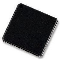
ADSP-BF592KCPZ Analog Devices Inc, ADSP-BF592KCPZ Datasheet - Page 22

ADSP-BF592KCPZ
Manufacturer Part Number
ADSP-BF592KCPZ
Description
58T4522
Manufacturer
Analog Devices Inc
Specifications of ADSP-BF592KCPZ
Operating Temperature (min)
0C
Operating Temperature (max)
70C
Operating Temperature Classification
Commercial
Mounting
Surface Mount
Pin Count
64
Rohs Compliant
YES
Frequency
400MHz
Embedded Interface Type
PPI, SPI, UART
No. Of I/o's
32
Operating Temperature Range
0°C To +70°C
Digital Ic Case Style
LFCSP
No. Of Pins
64
Core Supply Voltage
1.4V
Lead Free Status / RoHS Status
Compliant
Available stocks
Company
Part Number
Manufacturer
Quantity
Price
Company:
Part Number:
ADSP-BF592KCPZ-2
Manufacturer:
BROADCOM
Quantity:
154
ADSP-BF592
ABSOLUTE MAXIMUM RATINGS
Stresses greater than those listed in
nent damage to the device. These are stress ratings only.
Functional operation of the device at these or any other condi-
tions greater than those indicated in the operational sections of
this specification is not implied. Exposure to absolute maximum
rating conditions for extended periods may affect device
reliability.
Table 16. Absolute Maximum Ratings
1
2
Table 17. Maximum Duty Cycle for Input Transient Voltage
1
2
3
Table 16
rent for a group of pins and for individual pins. Permanent
damage can occur if this value is exceeded. To understand this
specification, if pins PF0 and PF1 from Group 1 in the Total
Current Pin Groups-Vddext Groups table were sourcing or
sinking 10 mA each, the total current for those pins would be 20
mA. This would allow up to 35 mA total that could be sourced
or sunk by the remaining pins in the group without damaging
the device. It should also be noted that the maximum source or
sink current for an individual pin can not exceed 25 mA. For a
list of all groups and their pins, see
and V
requirements, see the
Parameter
Internal Supply Voltage (V
External (I/O) Supply Voltage (V
Input Voltage
Output Voltage Swing
I
I
Storage Temperature Range
Junction Temperature While Biased +110°C
V
–0.5
–0.7
–0.8
–0.9
–1.0
Applies to 100% transient duty cycle. For other duty cycles see
Applies only when V
Applies to all signal pins with the exception of CLKIN, XTAL, EXT_WAKE.
The individual values cannot be combined for analysis of a single instance of
Duty cycle refers to the percentage of time the signal exceeds the value for the
OH
OH
fications, the range is V
overshoot or undershoot. The worst case observed value must fall within one of
the voltages specified and the total duration of the overshoot or undershoot
(exceeding the 100% case) must be less than or equal to the corresponding duty
cycle.
100% case. The is equivalent to the measured duration of a single instance of
overshoot or undershoot as a percentage of the period of occurrence.
IN
/I
/I
Min (V)
OL
OL
OL
Current per Pin Group
Current per Individual Pin
specifications have separate per-pin maximum current
specifies the maximum total source/sink (I
2
1, 2
DDEXT
V
+3.8
+4.0
+4.1
+4.2
+4.3
IN
DDEXT
Max (V)
is within specifications. When V
Electrical Characteristics
± 0.2 Volts.
DDINT
2
)
DDEXT
Maximum Duty Cycle
100%
40%
25%
15%
10%
Table
Table 16
) –0.3 V to +3.8 V
Rating
1.16 V to +1.47 V
–0.5 V to +3.6 V
–0.5 V to V
25 mA (Max)
–65°C to +150°C
55 mA (Max)
18. Note that the V
may cause perma-
DDEXT
table.
DDEXT
Rev. PrC | Page 22 of 46 | August 2010
Table
is outside speci-
OH
+0.5 V
/I
17.
OL
3
) cur-
OH
1
Table 18. Total Current Pin Groups–V
ESD SENSITIVITY
PACKAGE INFORMATION
The information presented in
details about the package branding for the ADSP-BF592 proces-
sor. For a complete listing of product availability, see
Guide on Page
Group
1
2
3
4
5
6
7
8
9
10
11
12
Pins in Group
PF0, PF1, PF2, PF3
PF4, PF5, PF6, PF7
PF8, PF9, PF10, PF11
PF12, PF13, PF14, PF15
PG3, PG2, PG1, PG0
PG7, PG6, PG5, PG4
PG11, PG10, PG9, PG8
PG15, PG14, PG13, PG12
TDI, TDO, EMU, TCK, TRST, TMS
BMODE2, BMODE1, BMODE0
EXT_WAKE, PG, RESET, NMI, PPI_CLK, CLKBUF
SDA, SCL, CLKIN, XTAL
Figure 6. Product Information on Package
45.
ESD (electrostatic discharge) sensitive device.
Charged devices and circuit boards can discharge
without detection. Although this product features
patented or proprietary circuitry, damage may occur
on devices subjected to high energy ESD. Therefore,
proper ESD precautions should be taken to avoid
performance degradation or loss of functionality.
Preliminary Technical Data
#yyww country_of_origin
ADSP-BF59x
vvvvvv.x n.n
tppZccc
Figure 6
and
DDEXT
Table 19
Groups
provides
Ordering


