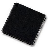
ADSP-BF592KCPZ Analog Devices Inc, ADSP-BF592KCPZ Datasheet - Page 9

ADSP-BF592KCPZ
Manufacturer Part Number
ADSP-BF592KCPZ
Description
58T4522
Manufacturer
Analog Devices Inc
Specifications of ADSP-BF592KCPZ
Operating Temperature (min)
0C
Operating Temperature (max)
70C
Operating Temperature Classification
Commercial
Mounting
Surface Mount
Pin Count
64
Rohs Compliant
YES
Frequency
400MHz
Embedded Interface Type
PPI, SPI, UART
No. Of I/o's
32
Operating Temperature Range
0°C To +70°C
Digital Ic Case Style
LFCSP
No. Of Pins
64
Core Supply Voltage
1.4V
Lead Free Status / RoHS Status
Compliant
Available stocks
Company
Part Number
Manufacturer
Quantity
Price
Company:
Part Number:
ADSP-BF592KCPZ-2
Manufacturer:
BROADCOM
Quantity:
154
Preliminary Technical Data
SERIAL PERIPHERAL INTERFACE (SPI) PORTS
The processors have two SPI-compatible ports that enable the
processor to communicate with multiple SPI-compatible
devices.
The SPI interface uses three pins for transferring data: two data
pins (Master Output-Slave Input, MOSI, and Master Input-
Slave Output, MISO) and a clock pin (serial clock, SCK). An SPI
chip select input pin (SPIx_SS) lets other SPI devices select the
processor, and many SPI chip select output pins (SPIx_SEL7–1)
let the processor select other SPI devices. The SPI select pins are
reconfigured general-purpose I/O pins. Using these pins, the
SPI port provides a full-duplex, synchronous serial interface,
which supports both master/slave modes and multimaster
environments.
UART PORT
The ADSP-BF592 processor provides a full-duplex universal
asynchronous receiver/transmitter (UART) port, which is fully
compatible with PC-standard UARTs. The UART port provides
a simplified UART interface to other peripherals or hosts, sup-
porting full-duplex, DMA-supported, asynchronous transfers of
serial data. The UART port includes support for five to
eight data bits, one or two stop bits, and none, even, or odd par-
ity. The UART port supports two modes of operation:
PARALLEL PERIPHERAL INTERFACE (PPI)
The processor provides a parallel peripheral interface (PPI) that
can connect directly to parallel A/D and D/A converters, video
encoders and decoders, and other general-purpose peripherals.
The PPI consists of a dedicated input clock pin, up to three
frame synchronization pins, and up to 16 data pins. The input
clock supports parallel data rates up to half the system clock rate
and the synchronization signals can be configured as either
inputs or outputs.
• DMA operations with single-cycle overhead – Each SPORT
• Interrupts – Each transmit and receive port generates an
• Multichannel capability – Each SPORT supports 128 chan-
• PIO (programmed I/O) – The processor sends or receives
• DMA (direct memory access) – The DMA controller trans-
can automatically receive and transmit multiple buffers of
memory data. The processor can link or chain sequences of
DMA transfers between a SPORT and memory.
interrupt upon completing the transfer of a data word or
after transferring an entire data buffer, or buffers,
through DMA.
nels out of a 1024-channel window and is compatible with
the H.100, H.110, MVIP-90, and HMVIP standards.
data by writing or reading I/O mapped UART registers.
The data is double-buffered on both transmit and receive.
fers both transmit and receive data. This reduces the
number and frequency of interrupts required to transfer
data to and from memory. The UART has two dedicated
DMA channels, one for transmit and one for receive. These
DMA channels have lower default priority than most DMA
channels because of their relatively low service rates.
Rev. PrC | Page 9 of 46 | August 2010
The PPI supports a variety of general-purpose and ITU-R 656
modes of operation. In general-purpose mode, the PPI provides
half-duplex, bidirectional data transfer with up to 16 bits of
data. Up to three frame synchronization signals are also pro-
vided. In ITU-R 656 mode, the PPI provides half-duplex
bidirectional transfer of 8- or 10-bit video data. Additionally,
on-chip decode of embedded start-of-line (SOL) and start-of-
field (SOF) preamble packets is supported.
General-Purpose Mode Descriptions
The general-purpose modes of the PPI are intended to suit a
wide variety of data capture and transmission applications.
Three distinct submodes are supported:
Input Mode
Input mode is intended for ADC applications, as well as video
communication with hardware signaling. In its simplest form,
PPI_FS1 is an external frame sync input that controls when to
read data. The PPI_DELAY MMR allows for a delay (in
PPI_CLK cycles) between reception of this frame sync and the
initiation of data reads. The number of input data samples is
user programmable and defined by the contents of the
PPI_COUNT register. The PPI supports 8-bit and 10-bit
through 16-bit data, programmable in the PPI_CONTROL
register.
Frame Capture Mode
Frame capture mode allows the video source(s) to act as a slave
(for frame capture for example). The ADSP-BF592 processor
controls when to read from the video source(s). PPI_FS1 is an
HSYNC output and PPI_FS2 is a VSYNC output.
Output Mode
Output mode is used for transmitting video or other data with
up to three output frame syncs. Typically, a single frame sync is
appropriate for data converter applications, whereas two or
three frame syncs could be used for sending video with hard-
ware signaling.
ITU-R 656 Mode Descriptions
The ITU-R 656 modes of the PPI are intended to suit a wide
variety of video capture, processing, and transmission applica-
tions. Three distinct submodes are supported:
Active Video Mode
Active video only mode is used when only the active video por-
tion of a field is of interest and not any of the blanking intervals.
The PPI does not read in any data between the end of active
• Input mode – Frame syncs and data are inputs into the PPI.
• Frame capture mode – Frame syncs are outputs from the
• Output mode – Frame syncs and data are outputs from the
• Active video only mode
• Vertical blanking only mode
• Entire field mode
PPI, but data are inputs.
PPI.
ADSP-BF592


