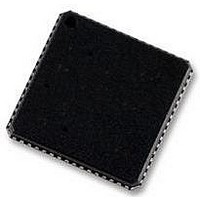
ADSP-BF592KCPZ Analog Devices Inc, ADSP-BF592KCPZ Datasheet - Page 13

ADSP-BF592KCPZ
Manufacturer Part Number
ADSP-BF592KCPZ
Description
58T4522
Manufacturer
Analog Devices Inc
Specifications of ADSP-BF592KCPZ
Operating Temperature (min)
0C
Operating Temperature (max)
70C
Operating Temperature Classification
Commercial
Mounting
Surface Mount
Pin Count
64
Rohs Compliant
YES
Frequency
400MHz
Embedded Interface Type
PPI, SPI, UART
No. Of I/o's
32
Operating Temperature Range
0°C To +70°C
Digital Ic Case Style
LFCSP
No. Of Pins
64
Core Supply Voltage
1.4V
Lead Free Status / RoHS Status
Compliant
Available stocks
Company
Part Number
Manufacturer
Quantity
Price
Company:
Part Number:
ADSP-BF592KCPZ-2
Manufacturer:
BROADCOM
Quantity:
154
Preliminary Technical Data
Note that the divisor ratio must be chosen to limit the system
clock frequency to its maximum of f
changed dynamically without any PLL lock latencies by writing
the appropriate values to the PLL divisor register (PLL_DIV).
The core clock (CCLK) frequency can also be dynamically
changed by means of the CSEL1–0 bits of the PLL_DIV register.
Supported CCLK divider ratios are 1, 2, 4, and 8, as shown in
Table
fast core frequency modifications.
Table 7. Core Clock Ratios
Table 6. Example System Clock Ratios
The maximum CCLK frequency both depends on the part’s
instruction rate (see
V
clock rate (SCLK) depends on the chip package and the applied
V
BOOTING MODES
The processor has several mechanisms (listed in
automatically loading internal and external memory after a
reset. The boot mode is defined by the BMODE input pins dedi-
cated to this purpose. There are two categories of boot modes.
Signal Name
CSEL1–0
00
01
10
11
Signal Name
SSEL3–0
0010
0110
1010
DDINT
DDINT
CLKIN
7. This programmable core clock capability is useful for
voltage. See
and V
REQUIRES PLL SEQUENCING
DDEXT
“FINE” ADJUSTMENT
Figure 5. Frequency Modification Methods
5u to 64u
Divider Ratio
VCO/CCLK
1:1
2:1
4:1
8:1
Divider Ratio
VCO/SCLK
2:1
6:1
10:1
PLL
voltages (see
Table 10
Page
45) and depends on the applied
for details. The maximal system
SCLK d CCLK
VCO
Table
Example Frequency Ratios
(MHz)
VCO
300
300
400
200
Example Frequency Ratios
(MHz)
VCO
100
300
400
SCLK
12).
. The SSEL value can be
“COARSE” ADJUSTMENT
÷ TBD
÷ TBD
ON-THE-FLY
Table
CCLK
300
150
100
25
SCLK
50
50
40
Rev. PrC | Page 13 of 46 | August 2010
8) for
CCLK
SCLK
In master boot modes, the processor actively loads data from
parallel or serial memories. In slave boot modes, the processor
receives data from external host devices.
Table 8. Booting Modes
The boot modes listed in
nisms for automatically loading the processor’s internal and
external memories after a reset. By default, all boot modes use
the slowest meaningful configuration settings. Default settings
can be altered via the initialization code feature at boot time.
The BMODE pins of the reset configuration register, sampled
during power-on resets and software-initiated resets, imple-
ment the modes shown in
BMODE2–0 Description
000
001
010
011
100
101
110
111
• IDLE State / No Boot (BMODE - 0x0) — In this mode, the
• SPI1 master boot from flash (BMODE = 0x2) — In this
• SPI1 slave boot from external master (BMODE = 0x3) — In
• SPI0 master boot from flash (BMODE = 0x4) — In this
boot kernel transitions the processor into Idle state. The
processor can then be controlled through JTAG for recov-
ery, debug, or other functions.
mode SPI1 is configured to operate in master mode and to
connect to 8-, 16-, 24-, or 32-bit addressable devices. The
processor uses the PG11/SPI1_SSEL5 to select a single SPI
EEPROM/flash device, submits a read command and suc-
cessive address bytes (0×00) until a valid 8-, 16-, 24-, or 32-
bit addressable device is detected, and begins clocking data
into the processor. Pull-up resistors are required on the
SSEL and MISO pins. By default, a value of 0×85 is written
to the SPI_BAUD register.
this mode SPI1 is configured to operate in slave mode and
to receive the bytes of the .LDR file from a SPI host (mas-
ter) agent. To hold off the host device from transmitting
while the boot ROM is busy, the Blackfin processor asserts
a GPIO pin, called host wait (HWAIT), to signal to the host
device not to send any more bytes until the pin is deas-
serted. The host must interrogate the HWAIT signal,
available on PF4, before transmitting every data unit to the
processor. A pull-up resistor is required on the SPI1_SS
input. A pull-down on the serial clock may improve signal
quality and booting robustness.
mode SPI0 is configured to operate in master mode and to
connect to 8-, 16-, 24-, or 32-bit addressable devices. The
processor uses the PF8/SPI0_SSEL2 to select a single SPI
EEPROM/flash device, submits a read command and suc-
cessive address bytes (0×00) until a valid 8-, 16-, 24-, or 32-
Idle/No Boot
Reserved
SPI1 master boot from Flash, using SPI1_SSEL5 on PG11
SPI1 slave boot from external master
SPI0 master boot from Flash, using SPI0_SSEL2 on PF8
Boot from PPI port
Boot from UART host device
Execute from Internal L1 ROM
Table 8
Table
8.
provide a number of mecha-
ADSP-BF592


