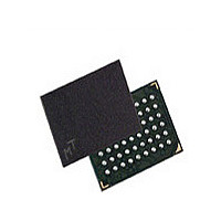
MT45W256KW16BEGB-708 WT Micron Technology Inc, MT45W256KW16BEGB-708 WT Datasheet - Page 14

MT45W256KW16BEGB-708 WT
Manufacturer Part Number
MT45W256KW16BEGB-708 WT
Description
Manufacturer
Micron Technology Inc
Datasheet
1.MT45W256KW16BEGB-708_WT.pdf
(58 pages)
Specifications of MT45W256KW16BEGB-708 WT
Operating Temperature (max)
85C
Mounting
Surface Mount
Operating Temperature Classification
Commercial
Lead Free Status / Rohs Status
Compliant
- Current page: 14 of 58
- Download datasheet (2Mb)
Figure 9:
Mixed-Mode Operation
PDF: 09005aef8329f3e3 / Source: 09005aef82e419a5
8mb_4mb_burst_cr1_0_p22z__2.fm - Rev. B 4/ 08 EN
Burst Mode WRITE (4-Word Burst)
DQ[15:0]
LB#/UB#
A[17:0]
ADV#
WAIT
WE#
OE#
CLK
CE#
Note:
The device can support a combination of synchronous READ and asynchronous WRITE
operations when the BCR is configured for synchronous operation. The asynchronous
WRITE operation requires that the clock (CLK) be held static LOW or HIGH during the
entire sequence. The ADV# signal can be used to latch the target address, or it can
remain LOW during the entire WRITE operation. CE# must return HIGH when transi-
tioning between mixed-mode operations. Note that the
READ or WRITE cycle. This time is required to ensure adequate refresh. Mixed-mode
operation facilitates a seamless interface to legacy burst mode Flash memory controllers
(see Figure 43 on page 51).
WRITE burst Identified
Nondefault BCR settings: latency code 2 (3 clocks); WAIT active LOW; WAIT asserted during
delay.
(WE# = LOW)
Address
valid
4Mb: 256K x 16 Async/Page/Burst CellularRAM 1.0 Memory
Latency code 2 (3 clocks)
14
D[0]
Micron Technology, Inc., reserves the right to change products or specifications without notice.
D[1]
t
CKA period is the same as a
D[2]
Bus Operating Modes
©2008 Micron Technology, Inc. All rights reserved.
Don’t Care
D[3]
Related parts for MT45W256KW16BEGB-708 WT
Image
Part Number
Description
Manufacturer
Datasheet
Request
R

Part Number:
Description:
IC SDRAM 64MBIT 133MHZ 54TSOP
Manufacturer:
Micron Technology Inc
Datasheet:

Part Number:
Description:
IC SDRAM 64MBIT 5.5NS 86TSOP
Manufacturer:
Micron Technology Inc
Datasheet:

Part Number:
Description:
IC SDRAM 64MBIT 200MHZ 86TSOP
Manufacturer:
Micron Technology Inc
Datasheet:

Part Number:
Description:
IC SDRAM 64MBIT 133MHZ 54TSOP
Manufacturer:
Micron Technology Inc
Datasheet:

Part Number:
Description:
IC SDRAM 128MBIT 133MHZ 54TSOP
Manufacturer:
Micron Technology Inc
Datasheet:

Part Number:
Description:
IC SDRAM 256MBIT 133MHZ 90VFBGA
Manufacturer:
Micron Technology Inc
Datasheet:

Part Number:
Description:
IC SDRAM 128MBIT 133MHZ 54TSOP
Manufacturer:
Micron Technology Inc
Datasheet:

Part Number:
Description:
IC SDRAM 256MBIT 133MHZ 54TSOP
Manufacturer:
Micron Technology Inc
Datasheet:

Part Number:
Description:
IC DDR SDRAM 512MBIT 6NS 66TSOP
Manufacturer:
Micron Technology Inc
Datasheet:

Part Number:
Description:
IC SDRAM 128MBIT 167MHZ 86TSOP
Manufacturer:
Micron Technology Inc
Datasheet:

Part Number:
Description:
IC SDRAM 128MBIT 143MHZ 86TSOP
Manufacturer:
Micron Technology Inc
Datasheet:

Part Number:
Description:
SDRAM 256M-BIT 1.8V 54-PIN VFBGA
Manufacturer:
Micron Technology Inc
Datasheet:

Part Number:
Description:
IC SDRAM 128MBIT 143MHZ 86TSOP
Manufacturer:
Micron Technology Inc
Datasheet:

Part Number:
Description:
IC SDRAM 128MBIT 125MHZ 54VFBGA
Manufacturer:
Micron Technology Inc
Datasheet:

Part Number:
Description:
IC SDRAM 128MBIT 125MHZ 54VFBGA
Manufacturer:
Micron Technology Inc
Datasheet:


