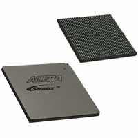
EP1S80B956C7N Altera, EP1S80B956C7N Datasheet - Page 440

EP1S80B956C7N
Manufacturer Part Number
EP1S80B956C7N
Description
IC STRATIX FPGA 80K LE 956-BGA
Manufacturer
Altera
Series
Stratix®r
Datasheet
1.EP1S10F484I6N.pdf
(864 pages)
Specifications of EP1S80B956C7N
Number Of Logic Elements/cells
79040
Number Of Labs/clbs
7904
Total Ram Bits
7427520
Number Of I /o
683
Voltage - Supply
1.425 V ~ 1.575 V
Mounting Type
Surface Mount
Operating Temperature
0°C ~ 85°C
Package / Case
956-BGA
Lead Free Status / RoHS Status
Lead free / RoHS Compliant
Number Of Gates
-
Available stocks
Company
Part Number
Manufacturer
Quantity
Price
- Current page: 440 of 864
- Download datasheet (11Mb)
Stratix & Stratix GX I/O Standards
Figure 4–13. Differential SSTL-2 Class II Termination
4–12
Stratix Device Handbook, Volume 2
Transmitter
Differential
25 Ω
25 Ω
50 Ω
standard and supplements the SSTL-2 standard for differential clocks.
The differential SSTL-2 standard specifies an input voltage range of
– 0.3 V V
require an input reference voltage differential. See
on differential SSTL-2 termination. Stratix and Stratix GX devices support
output clock levels for differential SSTL-2 Class II operation. The output
clock is implemented using two single-ended output buffers which are
programmed to have opposite polarity.
LVDS - ANSI/TIA/EIA Standard ANSI/TIA/EIA-644
The LVDS I/O standard is a differential high-speed, low-voltage swing,
low-power, general-purpose I/O interface standard requiring a 3.3-V
V
data transfer, backplane drivers, and clock distribution. The
ANSI/TIA/EIA-644 standard specifies LVDS transmitters and receivers
capable of operating at recommended maximum data signaling rates of
655 Mbps. However, devices can operate at slower speeds if needed, and
there is a theoretical maximum of 1.923 Gbps. Stratix and Stratix GX
devices meet the ANSI/TIA/EIA-644 standard.
Due to the low voltage swing of the LVDS I/O standard, the
electromagnetic interference (EMI) effects are much smaller than CMOS,
TTL, and PECL. This low EMI makes LVDS ideal for applications with
low EMI requirements or noise immunity requirements. The LVDS
standard does not require an input reference voltage, however, it does
require a 100
buffer. Stratix and Stratix GX devices include an optional differential
LVDS termination resistor within the device using differential on-chip
termination. Stratix and Stratix GX devices support both input and
output levels.
V
CCIO
TT
= 1.25 V
. This standard is used in applications requiring high-bandwidth
I
50 Ω
V
V
TT
CCIO
termination resistor between the two signals at the input
= 1.25 V
+ 0.3 V. The differential SSTL-2 standard does not
Z
Z
0
0
= 50 Ω
= 50 Ω
50 Ω
V
TT
= 1.25 V
50 Ω
V
TT
= 1.25 V
Figure 4–13
Altera Corporation
Differential
Receiver
for details
June 2006
Related parts for EP1S80B956C7N
Image
Part Number
Description
Manufacturer
Datasheet
Request
R

Part Number:
Description:
CYCLONE II STARTER KIT EP2C20N
Manufacturer:
Altera
Datasheet:

Part Number:
Description:
CPLD, EP610 Family, ECMOS Process, 300 Gates, 16 Macro Cells, 16 Reg., 16 User I/Os, 5V Supply, 35 Speed Grade, 24DIP
Manufacturer:
Altera Corporation
Datasheet:

Part Number:
Description:
CPLD, EP610 Family, ECMOS Process, 300 Gates, 16 Macro Cells, 16 Reg., 16 User I/Os, 5V Supply, 15 Speed Grade, 24DIP
Manufacturer:
Altera Corporation
Datasheet:

Part Number:
Description:
Manufacturer:
Altera Corporation
Datasheet:

Part Number:
Description:
CPLD, EP610 Family, ECMOS Process, 300 Gates, 16 Macro Cells, 16 Reg., 16 User I/Os, 5V Supply, 30 Speed Grade, 24DIP
Manufacturer:
Altera Corporation
Datasheet:

Part Number:
Description:
High-performance, low-power erasable programmable logic devices with 8 macrocells, 10ns
Manufacturer:
Altera Corporation
Datasheet:

Part Number:
Description:
High-performance, low-power erasable programmable logic devices with 8 macrocells, 7ns
Manufacturer:
Altera Corporation
Datasheet:

Part Number:
Description:
Classic EPLD
Manufacturer:
Altera Corporation
Datasheet:

Part Number:
Description:
High-performance, low-power erasable programmable logic devices with 8 macrocells, 10ns
Manufacturer:
Altera Corporation
Datasheet:

Part Number:
Description:
Manufacturer:
Altera Corporation
Datasheet:

Part Number:
Description:
Manufacturer:
Altera Corporation
Datasheet:

Part Number:
Description:
Manufacturer:
Altera Corporation
Datasheet:

Part Number:
Description:
CPLD, EP610 Family, ECMOS Process, 300 Gates, 16 Macro Cells, 16 Reg., 16 User I/Os, 5V Supply, 25 Speed Grade, 24DIP
Manufacturer:
Altera Corporation
Datasheet:


