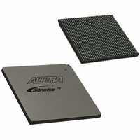
EP1S80B956C7N Altera, EP1S80B956C7N Datasheet - Page 478

EP1S80B956C7N
Manufacturer Part Number
EP1S80B956C7N
Description
IC STRATIX FPGA 80K LE 956-BGA
Manufacturer
Altera
Series
Stratix®r
Datasheet
1.EP1S10F484I6N.pdf
(864 pages)
Specifications of EP1S80B956C7N
Number Of Logic Elements/cells
79040
Number Of Labs/clbs
7904
Total Ram Bits
7427520
Number Of I /o
683
Voltage - Supply
1.425 V ~ 1.575 V
Mounting Type
Surface Mount
Operating Temperature
0°C ~ 85°C
Package / Case
956-BGA
Lead Free Status / RoHS Status
Lead free / RoHS Compliant
Number Of Gates
-
Available stocks
Company
Part Number
Manufacturer
Quantity
Price
- Current page: 478 of 864
- Download datasheet (11Mb)
Principles of SERDES Operation
Principles of
SERDES
Operation
5–6
Stratix Device Handbook, Volume 2
signaling, you can configure them as any of the other supported I/O
standards. DDRIO capabilities are detailed in
Differential Signaling”
Stratix devices support source-synchronous differential signaling up to
840 Mbps. Serial data is transmitted and received along with a low-
frequency clock. The PLL can multiply the incoming low-frequency clock
by a factor of 1 to 10. The SERDES factor J can be 4, 7, 8, or 10 and does not
have to equal the clock multiplication value.
possible by bypassing the SERDES; it is explained in
DDR Differential Interface Review”
On the receiver side, the high-frequency clock generated by the PLL shifts
the serial data through a shift register (also called deserializer). The
parallel data is clocked out to the logic array synchronized with the low-
frequency clock. On the transmitter side, the parallel data from the logic
array is first clocked into a parallel-in, serial-out shift register
synchronized with the low-frequency clock and then transmitted out by
the output buffers.
There are four dedicated fast PLLs in EP1S10 to EP1S25 devices, and eight
in EP1S30 to EP1S80 devices. These PLLs are used for the SERDES
operations as well as general-purpose use.
The differential channels and the high-speed PLL layout in Stratix
devices are described in the
section on
Note to
(1)
Left
Right
Top
Bottom
Device Side
Table 5–1. I/O Pin Locations on Each Side of Stratix Devices
Device sides are relative to pin A1 in the upper left corner of the device (top view
of the package).
Table
page
(1)
5–1:
5–16.
Differential Input
on
v
v
page
“Differential I/O Interface & Fast PLLs”
5–42.
on
page
Differential Output
5–42.
×
“SERDES Bypass DDR
1 and
v
v
×
“SERDES Bypass
2 operation is also
Altera Corporation
DDRIO
July 2005
v
v
v
v
Related parts for EP1S80B956C7N
Image
Part Number
Description
Manufacturer
Datasheet
Request
R

Part Number:
Description:
CYCLONE II STARTER KIT EP2C20N
Manufacturer:
Altera
Datasheet:

Part Number:
Description:
CPLD, EP610 Family, ECMOS Process, 300 Gates, 16 Macro Cells, 16 Reg., 16 User I/Os, 5V Supply, 35 Speed Grade, 24DIP
Manufacturer:
Altera Corporation
Datasheet:

Part Number:
Description:
CPLD, EP610 Family, ECMOS Process, 300 Gates, 16 Macro Cells, 16 Reg., 16 User I/Os, 5V Supply, 15 Speed Grade, 24DIP
Manufacturer:
Altera Corporation
Datasheet:

Part Number:
Description:
Manufacturer:
Altera Corporation
Datasheet:

Part Number:
Description:
CPLD, EP610 Family, ECMOS Process, 300 Gates, 16 Macro Cells, 16 Reg., 16 User I/Os, 5V Supply, 30 Speed Grade, 24DIP
Manufacturer:
Altera Corporation
Datasheet:

Part Number:
Description:
High-performance, low-power erasable programmable logic devices with 8 macrocells, 10ns
Manufacturer:
Altera Corporation
Datasheet:

Part Number:
Description:
High-performance, low-power erasable programmable logic devices with 8 macrocells, 7ns
Manufacturer:
Altera Corporation
Datasheet:

Part Number:
Description:
Classic EPLD
Manufacturer:
Altera Corporation
Datasheet:

Part Number:
Description:
High-performance, low-power erasable programmable logic devices with 8 macrocells, 10ns
Manufacturer:
Altera Corporation
Datasheet:

Part Number:
Description:
Manufacturer:
Altera Corporation
Datasheet:

Part Number:
Description:
Manufacturer:
Altera Corporation
Datasheet:

Part Number:
Description:
Manufacturer:
Altera Corporation
Datasheet:

Part Number:
Description:
CPLD, EP610 Family, ECMOS Process, 300 Gates, 16 Macro Cells, 16 Reg., 16 User I/Os, 5V Supply, 25 Speed Grade, 24DIP
Manufacturer:
Altera Corporation
Datasheet:


