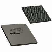
EP1S80B956C7N Altera, EP1S80B956C7N Datasheet - Page 769

EP1S80B956C7N
Manufacturer Part Number
EP1S80B956C7N
Description
IC STRATIX FPGA 80K LE 956-BGA
Manufacturer
Altera
Series
Stratix®r
Datasheet
1.EP1S10F484I6N.pdf
(864 pages)
Specifications of EP1S80B956C7N
Number Of Logic Elements/cells
79040
Number Of Labs/clbs
7904
Total Ram Bits
7427520
Number Of I /o
683
Voltage - Supply
1.425 V ~ 1.575 V
Mounting Type
Surface Mount
Operating Temperature
0°C ~ 85°C
Package / Case
956-BGA
Lead Free Status / RoHS Status
Lead free / RoHS Compliant
Number Of Gates
-
Available stocks
Company
Part Number
Manufacturer
Quantity
Price
- Current page: 769 of 864
- Download datasheet (11Mb)
Configuring
Using the
MicroBlaster
Driver
Device
Configuration
Pins
Altera Corporation
July 2005
VCCSEL
PORSEL
Table 11–15. Dedicated Configuration Pins on the Stratix or Stratix GX Device
Pin Name
N/A
N/A
User Mode
The MicroBlaster
devices in an embedded environment using PS or FPP mode. The
MicroBlaster software driver supports a Raw Binary File (.rbf)
programming input file. The source code is developed for the Windows
NT operating system, although you can customize it to run on other
operating systems. For more information on the MicroBlaster software
driver, go to the Altera web site (www.altera.com).
The following tables describe the connections and functionality of all the
configuration related pins on the Stratix or Stratix GX device.
describes the dedicated configuration pins, which are required to be
connected properly on your board for successful configuration. Some of
these pins may not be required for your configuration schemes.
All
All
Configuration
Scheme
TM
Input
Input
software driver allows you to configure Altera
Pin Type
Dedicated input that selects which input buffer
is used on the configuration input pins;
nCONFIG
nCS
The
V
resistor that is always active.
A logic high (1.5-V, 1.8-V, 2.5-V, 3.3-V) selects
the 1.8-V/1.5-V input buffer, and a logic low
selects the 3.3-V/2.5-V input buffer. See the
“V
Dedicated input which selects between a POR
time of 2 ms or 100 ms. A logic high (1.5-V, 1.8-
V, 2.5-V, 3.3-V) selects a POR time of about 2
ms and a logic low selects POR time of about
100 ms.
The
V
resistor that is always active.
C C I N T
C C I N T
CCSEL
Configuring Stratix & Stratix GX Devices
VCCSEL
PORSEL
and
and has an internal 2.5 k pull-down
Pins”
and has an internal 2.5 k pull-down
Stratix Device Handbook, Volume 2
CLKUSR
,
DCLK
input buffer is powered by
input buffer is powered by
section for more details.
,
Description
RUnLU
.
(Part 1 of 8)
,
nCE
,
nWS
Table 11–15
,
nRS
11–51
,
CS
,
Related parts for EP1S80B956C7N
Image
Part Number
Description
Manufacturer
Datasheet
Request
R

Part Number:
Description:
CYCLONE II STARTER KIT EP2C20N
Manufacturer:
Altera
Datasheet:

Part Number:
Description:
CPLD, EP610 Family, ECMOS Process, 300 Gates, 16 Macro Cells, 16 Reg., 16 User I/Os, 5V Supply, 35 Speed Grade, 24DIP
Manufacturer:
Altera Corporation
Datasheet:

Part Number:
Description:
CPLD, EP610 Family, ECMOS Process, 300 Gates, 16 Macro Cells, 16 Reg., 16 User I/Os, 5V Supply, 15 Speed Grade, 24DIP
Manufacturer:
Altera Corporation
Datasheet:

Part Number:
Description:
Manufacturer:
Altera Corporation
Datasheet:

Part Number:
Description:
CPLD, EP610 Family, ECMOS Process, 300 Gates, 16 Macro Cells, 16 Reg., 16 User I/Os, 5V Supply, 30 Speed Grade, 24DIP
Manufacturer:
Altera Corporation
Datasheet:

Part Number:
Description:
High-performance, low-power erasable programmable logic devices with 8 macrocells, 10ns
Manufacturer:
Altera Corporation
Datasheet:

Part Number:
Description:
High-performance, low-power erasable programmable logic devices with 8 macrocells, 7ns
Manufacturer:
Altera Corporation
Datasheet:

Part Number:
Description:
Classic EPLD
Manufacturer:
Altera Corporation
Datasheet:

Part Number:
Description:
High-performance, low-power erasable programmable logic devices with 8 macrocells, 10ns
Manufacturer:
Altera Corporation
Datasheet:

Part Number:
Description:
Manufacturer:
Altera Corporation
Datasheet:

Part Number:
Description:
Manufacturer:
Altera Corporation
Datasheet:

Part Number:
Description:
Manufacturer:
Altera Corporation
Datasheet:

Part Number:
Description:
CPLD, EP610 Family, ECMOS Process, 300 Gates, 16 Macro Cells, 16 Reg., 16 User I/Os, 5V Supply, 25 Speed Grade, 24DIP
Manufacturer:
Altera Corporation
Datasheet:


